
 German
 Japanese
 Portuguese
 Korea
Korea
 Mexico
 Dutch
Dutch


Texas Instruments
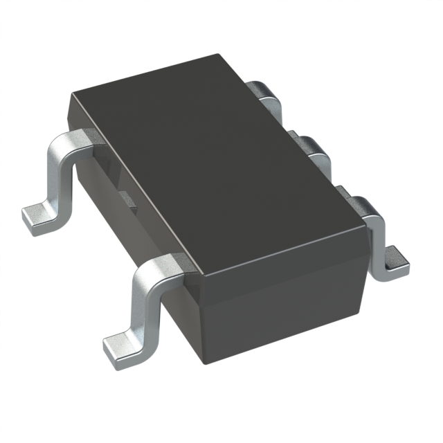
CLVC1G125QDBVRQ1

Why Choose Us?
Professional Platform
B2B & B2C purchasingDelivery at full speed
1-2 days deliveryWide variety
Original manufacturers365 days guarantee
Responsible quality
.png)


Tech Specifications
CLVC1G125QDBVRQ1 Description
The CLVC1G125QDBVRQ1 is a high-voltage, high-density programmable gate array (PGA) manufactured by Texas Instruments. It is designed to provide a flexible and customizable solution for a wide range of applications in the fields of industrial, medical, and automotive electronics.
Description:
The CLVC1G125QDBVRQ1 is a complex programmable logic device (CPLD) that offers a combination of digital logic, memory, and I/O capabilities in a single package. It is built using advanced CMOS technology and features a high-density architecture that allows for the implementation of large and complex digital designs.
Features:
- High-voltage operation: The CLVC1G125QDBVRQ1 can operate at supply voltages up to 5.5V, making it suitable for use in high-voltage applications.
- High-density architecture: The device offers a high-density architecture with up to 1,280 logic cells, providing ample resources for complex digital designs.
- Wide range of I/O options: The CLVC1G125QDBVRQ1 features a wide range of I/O options, including LVCMOS, LVDS, and HSTL, allowing for easy integration with various external components.
- On-chip memory: The device includes on-chip memory resources, such as block RAM and distributed RAM, which can be used for data storage and processing.
- In-system programmability: The CLVC1G125QDBVRQ1 can be programmed in-system, allowing for easy updates and modifications to the device's functionality.
- Low power consumption: The device is designed for low power consumption, making it suitable for battery-powered and energy-sensitive applications.
Applications:
The CLVC1G125QDBVRQ1 is a versatile device that can be used in a wide range of applications, including:
- Industrial control systems: The high-voltage operation and wide range of I/O options make the CLVC1G125QDBVRQ1 suitable for use in industrial control systems, such as motor control, sensor interfacing, and data acquisition.
- Medical electronics: The device's flexibility and programmability make it an ideal choice for medical electronics applications, such as patient monitoring systems, medical imaging, and diagnostic equipment.
- Automotive electronics: The CLVC1G125QDBVRQ1 can be used in various automotive applications, such as engine control, safety systems, and infotainment systems.
- Communication systems: The device's high-density architecture and LVDS I/O options make it suitable for use in high-speed communication systems, such as fiber-optic communication and high-speed data transmission.
- Custom computing applications: The CLVC1G125QDBVRQ1 can be used to implement custom computing solutions for specific applications, such as digital signal processing, cryptography, and custom control algorithms.
In summary, the Texas Instruments CLVC1G125QDBVRQ1 is a high-voltage, high-density programmable gate array that offers a flexible and customizable solution for a wide range of applications in industrial, medical, and automotive electronics. Its features, such as high-density architecture, on-chip memory, and in-system programmability, make it an ideal choice for complex digital designs and custom computing applications.
FAQ
| Quantity | Unit Price | Ext. Price |
|---|---|---|
| 5+ | $0.25452 | $1.27 |
| 50+ | $0.20300 | $10.15 |
| 150+ | $0.17788 | $26.68 |
| 500+ | $0.15545 | $77.73 |
Not available to buy online? Want the lower wholesale price? Please Send RFQ to get best price, we will respond immediately


.png?x-oss-process=image/format,webp/resize,h_32)


