
Texas Instruments
CLVC2G126MDCUTEP
Buffers, Drivers, Receivers, Transceivers


.png?x-oss-process=image/format,webp/resize,p_30)


CLVC2G126MDCUTEP Description
CLVC2G126MDCUTEP Description
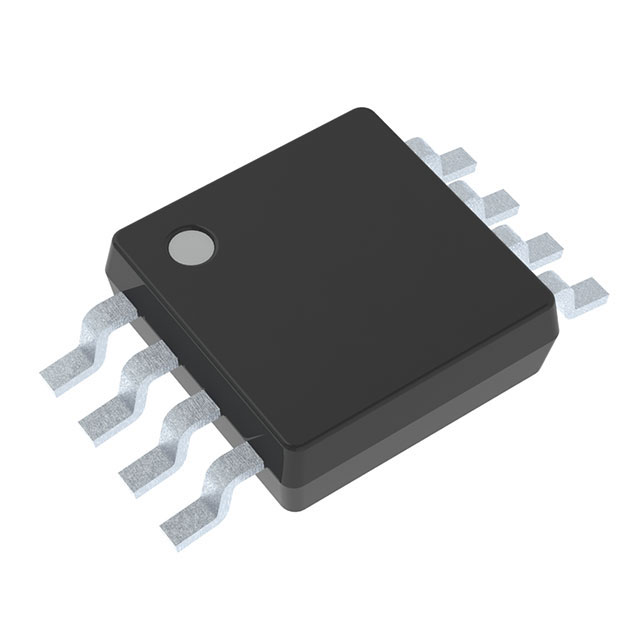
The CLVC2G126MDCUTEP is a high-performance, dual-channel buffer from Texas Instruments, designed to meet the demands of modern electronic systems. This IC features a 1.65V to 5.5V supply voltage range, making it suitable for a wide range of applications. With a surface-mount design, it is ideal for compact and space-constrained designs. The CLVC2G126MDCUTEP is RoHS3 compliant, REACH unaffected, and EAR99 classified, ensuring compliance with environmental and trade regulations.
CLVC2G126MDCUTEP Features
-
Technical Specifications:
- Number of Bits per Element: 1
- Voltage - Supply: 1.65V ~ 5.5V
- Current - Output High, Low: 32mA, 32mA
- Moisture Sensitivity Level (MSL): 1 (Unlimited)
- Number of Elements: 2
- Mounting Type: Surface Mount
- Package: Tape & Reel (TR)
-
Performance Benefits:
- Non-inverting operation for simple signal buffering
- Wide supply voltage range for compatibility with various power sources
- High output current capability for driving demanding loads
- Low power consumption for extended battery life in portable devices
-
Unique Features and Advantages:
- The CLVC2G126MDCUTEP offers a compact 8VSSOP package, making it an ideal choice for space-constrained applications.
- Its non-inverting operation simplifies circuit design and reduces the need for additional components.
- The wide supply voltage range allows for greater flexibility in system design and compatibility with various power sources.
CLVC2G126MDCUTEP Applications
The CLVC2G126MDCUTEP is ideal for a variety of applications where signal buffering and level translation are required. Some specific use cases include:
- Automotive Systems: For buffering and level translation in infotainment systems, sensor interfaces, and control modules.
- Industrial Control Systems: For signal conditioning and isolation in PLCs, motor controllers, and sensor interfaces.
- Communication Systems: For buffering and level translation in transceivers, routers, and switches.
- Consumer Electronics: For signal buffering in smartphones, tablets, and wearable devices.
Conclusion of CLVC2G126MDCUTEP
The CLVC2G126MDCUTEP is a versatile and high-performance dual-channel buffer from Texas Instruments. Its wide supply voltage range, compact package, and non-inverting operation make it an ideal choice for a variety of applications in automotive, industrial, communication, and consumer electronics. With its unique features and advantages, the CLVC2G126MDCUTEP offers a reliable and efficient solution for signal buffering and level translation in modern electronic systems.
Tech Specifications
CLVC2G126MDCUTEP Documents
Download datasheets and manufacturer documentation for CLVC2G126MDCUTEP
 SN74LVC2G126-EP
  SN74LVC2G126-EP
 Shopping Guide


.png?x-oss-process=image/format,webp/resize,h_32)


