
 German
 Japanese
 Portuguese
 Korea
Korea
 Mexico
 Dutch
Dutch


Texas Instruments
CSD16327Q3T
278-CSD16327Q3T

PDF Datasheet
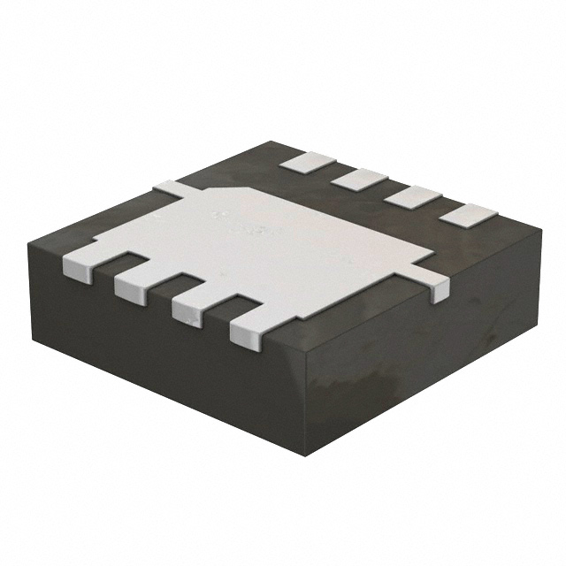
25V, N ch NexFET MOSFET™, single SON3x3, 4.8mOhm 8-VSON-CLIP -55 to 150
6 Weeks
Why Choose Us?
Professional Platform
B2B & B2C purchasingDelivery at full speed
1-2 days deliveryWide variety
Original manufacturers365 days guarantee
Responsible quality
.png)


Tech Specifications
Number of Terminals
5
Terminal Position
DUAL
Number of Elements
1
RoHS
No
Lead Free
Yes
REACH
not_compliant
Military Spec
False
CSD16327Q3T Description
N-Channel 25 V 60A (Tc) 74W (Tc) Surface Mount 8-VSON-CLIP (3.3x3.3)
FAQ
What is CSD16327Q3T?
CSD16327Q3T is a Single FETs, MOSFETs from Texas Instruments. This product page provides its main specifications, pricing information, availability, and inquiry options.
Is CSD16327Q3T currently in stock?
Does CSD16327Q3T have quantity-based pricing?
What is the standard lead time for CSD16327Q3T?
Are there related or alternative parts for CSD16327Q3T?
Availability
(In Stock :
6 )
| Quantity | Unit Price | Ext. Price |
|---|---|---|
| 1+ | $0.64115 | $0.64 |
| 10+ | $0.62743 | $6.27 |
| 30+ | $0.61715 | $18.51 |
Quick Quote
ADD TO RFQ LIST
Not available to buy online? Want the lower wholesale price? Please Send RFQ to get best price, we will respond immediately
QUICK RFQ


.png?x-oss-process=image/format,webp/resize,h_32)


