
 German
 Japanese
 Portuguese
 Korea
Korea
 Mexico
 Dutch
Dutch


Texas Instruments
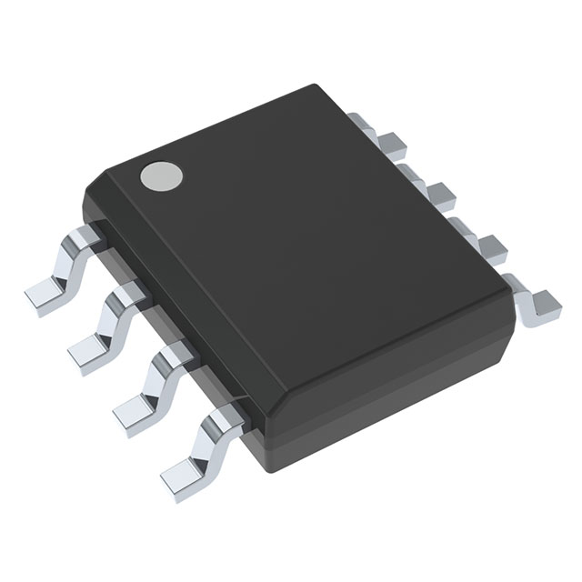
INA143UA

Why Choose Us?
Professional Platform
B2B & B2C purchasingDelivery at full speed
1-2 days deliveryWide variety
Original manufacturers365 days guarantee
Responsible quality
.png)


Tech Specifications
INA143UA Description
INA143UA Description
The INA143UA is a high-performance differential amplifier designed by Texas Instruments, suitable for a wide range of industrial and commercial applications. This Linear IC Chip features an 8SOIC package, making it ideal for surface mount applications where space is a premium. The INA143UA is currently in the "Last Time Buy" product status, indicating that it is a reliable choice for existing designs but may not be available for future projects.
INA143UA Features
- Supply Voltage Range: The INA143UA operates within a supply voltage range of 4.5 V to 36 V, offering flexibility in power supply requirements.
- Bandwidth: With a -3dB bandwidth of 150 kHz, the INA143UA ensures high-frequency performance, making it suitable for applications requiring fast signal processing.
- Slew Rate: The 5V/µs slew rate allows for rapid response to input signal changes, ensuring minimal distortion in high-frequency applications.
- Supply Current: The low supply current of 950µA minimizes power consumption, making the INA143UA energy-efficient.
- Output Current: The amplifier can deliver up to 32 mA per channel, providing robust output capabilities.
- Input Offset Voltage: The low input offset voltage of 100 µV ensures high accuracy and precision in differential signal measurements.
- Compliance and Packaging: The INA143UA is REACH unaffected and ROHS3 compliant, ensuring environmental safety and regulatory compliance. It is packaged in a tube, facilitating easy handling and storage.
- Moisture Sensitivity Level: With an MSL of 3 (168 Hours), the INA143UA is suitable for environments with moderate humidity, ensuring reliability and durability.
INA143UA Applications
The INA143UA is ideal for applications requiring high-precision differential signal amplification. Its wide supply voltage range and low supply current make it suitable for battery-powered devices and industrial control systems. The high slew rate and bandwidth ensure it can handle fast-changing signals, making it ideal for applications such as:
- Industrial Automation: For precise control and monitoring of industrial processes.
- Medical Equipment: For accurate signal processing in medical devices.
- Automotive Systems: For reliable performance in automotive electronic control units.
- Signal Conditioning: For amplifying and conditioning differential signals in various electronic systems.
Conclusion of INA143UA
The INA143UA from Texas Instruments is a versatile differential amplifier that offers a combination of high performance and energy efficiency. Its wide supply voltage range, low supply current, and high slew rate make it suitable for a variety of applications. The low input offset voltage ensures high accuracy, making it an excellent choice for precision signal processing. While it is currently in the "Last Time Buy" status, the INA143UA remains a reliable and high-performance option for existing designs.
FAQ
Not available to buy online? Want the lower wholesale price? Please Send RFQ to get best price, we will respond immediately


.png?x-oss-process=image/format,webp/resize,h_32)


