
Texas Instruments
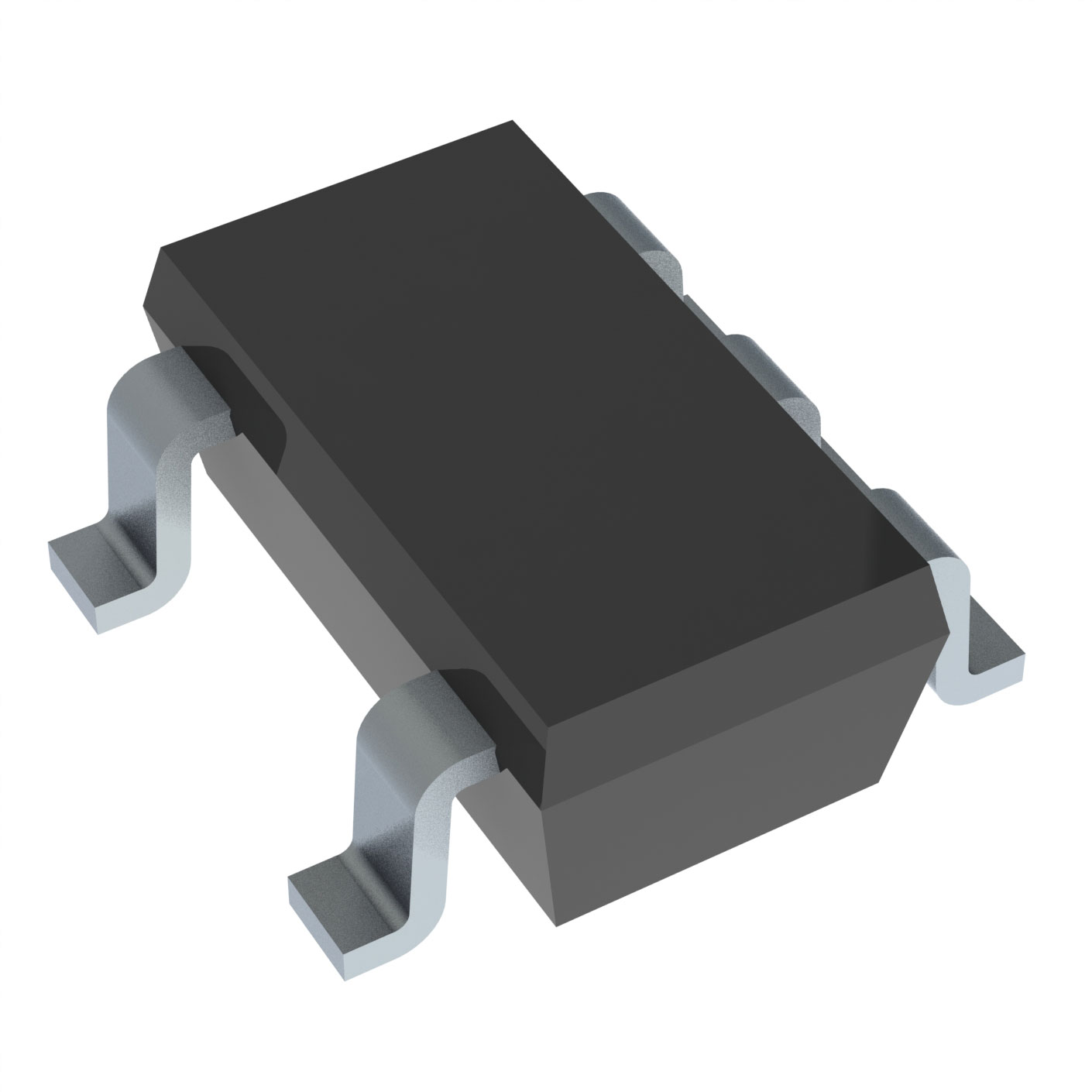
INA180A3IDBVR
OP Amps, Buffer Amps ICs


- 5+
- $0.20342
- $1.02
- 50+
- $0.16057
- $8.03
- 150+
- $0.13963
- $20.94
- 500+
- $0.12097
- $60.48
- 3000+
- $0.11585
- $347.55
- 6000+
- $0.11277
- $676.62

.png?x-oss-process=image/format,webp/resize,p_30)


INA180A3IDBVR Description
The INA180A3IDBVR is a monolithic, precision, low-power, instrumentation amplifier designed by Texas Instruments. This device is ideal for a wide range of applications, including medical, industrial, and automotive systems, where accurate and reliable signal conditioning is required.
Description:
The INA180A3IDBVR is a single, 8-pin, surface-mount package that provides a high level of precision and accuracy in signal conditioning. It is designed to amplify the difference between two input signals while rejecting common-mode interference. The device features a gain range of 1 to 1000, which can be easily set using an external feedback resistor network.
Features:
- Precision: The INA180A3IDBVR offers excellent precision with a maximum offset voltage drift of 0.5 µV/°C and a maximum input offset voltage of 25 µV.
- Low Power: The device operates with a low supply current of 40 µA, making it suitable for battery-powered applications.
- Wide Supply Voltage Range: The INA180A3IDBVR can operate with a supply voltage range of 2.7V to 10.6V, which allows for compatibility with various power sources.
- Programmable Gain: The gain can be easily set from 1 to 1000 using external feedback resistors, providing flexibility in system design.
- High Input Impedance: The device features high input impedance, which minimizes the loading effect on the input signal sources.
- Internal Frequency Compensation: The INA180A3IDBVR includes internal frequency compensation, eliminating the need for external components for stability.
- Robust Performance: The device is designed to provide reliable performance in various operating conditions, including temperature and supply voltage variations.
Applications:
- Medical Equipment: The INA180A3IDBVR can be used for amplifying and filtering signals from sensors in medical equipment, such as blood pressure monitors, pulse oximeters, and electrocardiogram (ECG) machines.
- Industrial Control Systems: The device can be utilized for signal conditioning in industrial control systems, where accurate and reliable signal processing is crucial.
- Automotive Applications: The INA180A3IDBVR can be used in automotive systems for processing signals from various sensors, such as pressure sensors, temperature sensors, and position sensors.
- Battery Monitoring Systems: The low-power consumption and high precision of the INA180A3IDBVR make it suitable for battery monitoring systems, where accurate voltage and current measurements are required.
- Strain Gauge Amplification: The device can be used to amplify signals from strain gauges in applications such as load cells and weigh scales.
- Data Acquisition Systems: The INA180A3IDBVR can be employed in data acquisition systems for amplifying and filtering signals from various sensors before digitization.
In summary, the INA180A3IDBVR from Texas Instruments is a versatile, precision, low-power instrumentation amplifier suitable for a wide range of applications where accurate signal conditioning is essential. Its features, such as programmable gain, low power consumption, and high input impedance, make it an attractive choice for designers working on projects in the medical, industrial, and automotive fields.
Tech Specifications
INA180A3IDBVR Documents
Download datasheets and manufacturer documentation for INA180A3IDBVR
 Assembly 28/Mar/2023
  INA180 Datasheet Current Sense Amplifiers Guide
 Shopping Guide


.png?x-oss-process=image/format,webp/resize,h_32)


