

Texas Instruments
INA293A4QDBVRQ1
OP Amps, Buffer Amps ICs

Not available to buy online? Want the lower wholesale price? Please Send RFQ to get best price, we will respond immediately


.png?x-oss-process=image/format,webp/resize,p_30)


INA293A4QDBVRQ1 Description
INA293A4QDBVRQ1 Description
The INA293A4QDBVRQ1 is a high-performance current sense amplifier designed for automotive applications, manufactured by Texas Instruments. This device is part of the INA293 family and is specifically tailored to meet the stringent requirements of the automotive industry. The INA293A4QDBVRQ1 features a wide supply voltage range from 2.7 V to 20 V, making it suitable for a variety of power supply configurations. It operates with a low input bias current of 20 µA and a supply current of 1.5 mA, ensuring minimal power consumption and high efficiency.
The device offers a -3 dB bandwidth of 900 kHz and a fast slew rate of 2.5 V/µs, enabling it to accurately measure high-frequency current signals. The INA293A4QDBVRQ1 also boasts a low input offset voltage of 5 µV, which is crucial for precise current sensing in low-voltage applications. Its automotive-grade qualification ensures reliability and robustness in demanding environments.
INA293A4QDBVRQ1 Features
- Wide Supply Voltage Range: Operates from 2.7 V to 20 V, providing flexibility for various power supply designs.
- Low Input Bias Current: 20 µA input bias current minimizes the impact on the measured current source.
- Low Input Offset Voltage: 5 µV input offset voltage ensures high accuracy in current sensing.
- High Bandwidth and Fast Slew Rate: 900 kHz bandwidth and 2.5 V/µs slew rate for accurate high-frequency measurements.
- Automotive Grade: Designed to meet the stringent requirements of automotive applications, ensuring reliability and robustness.
- Compliance: REACH unaffected and ROHS3 compliant, meeting environmental and regulatory standards.
- Moisture Sensitivity Level (MSL): MSL 1 (Unlimited) for ease of handling and assembly.
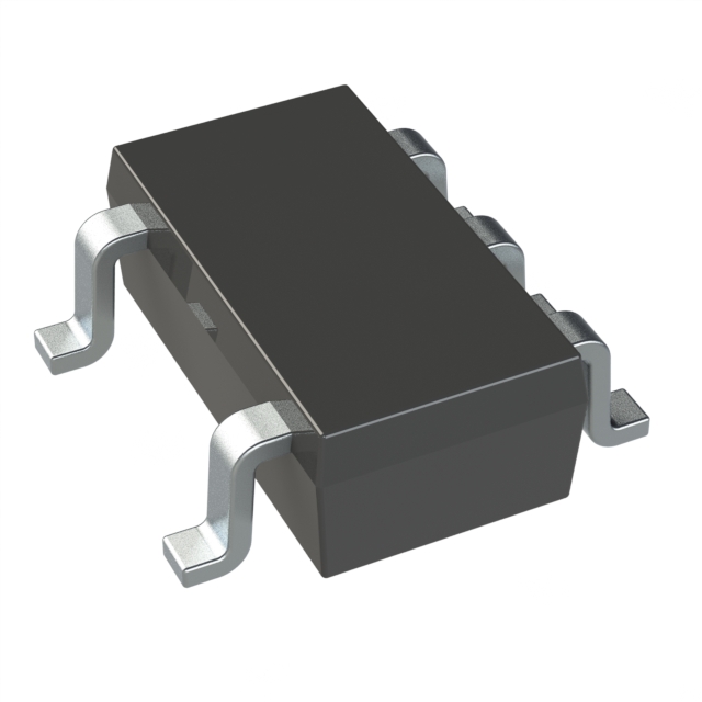
- Packaging: Available in a surface-mount SOT23-5 package, suitable for compact and space-constrained designs.
- Single Circuit Design: Simplifies integration and reduces complexity in system design.
INA293A4QDBVRQ1 Applications
The INA293A4QDBVRQ1 is ideal for a wide range of automotive applications where precise current sensing is critical. Some specific use cases include:
- Battery Management Systems: Accurate current sensing for monitoring battery charge and discharge cycles.
- Motor Control: Precise current measurement for efficient motor control and protection.
- Power Supply Monitoring: Ensuring stable power delivery and detecting overcurrent conditions.
- EV Charging Stations: Reliable current sensing for safe and efficient charging processes.
- Automotive Electronics: General-purpose current sensing in various electronic systems within the vehicle.
Conclusion of INA293A4QDBVRQ1
The INA293A4QDBVRQ1 from Texas Instruments stands out as a reliable and high-performance current sense amplifier tailored for automotive applications. Its wide supply voltage range, low input bias current, and low input offset voltage make it an excellent choice for precise current sensing in demanding environments. The device's compliance with automotive-grade standards ensures robustness and reliability, while its fast slew rate and high bandwidth enable accurate measurements of high-frequency signals. The INA293A4QDBVRQ1 is an ideal solution for engineers looking to integrate a high-precision current sense amplifier into their automotive designs, offering a balance of performance, efficiency, and compliance.
Tech Specifications
INA293A4QDBVRQ1 Documents
Download datasheets and manufacturer documentation for INA293A4QDBVRQ1
Product Change Notification 2024-02-05 (PDF) Product Change Notification (PDF) Related Parts


Shopping Guide


.png?x-oss-process=image/format,webp/resize,h_32)


©2025 ERSA Electronics Corporation.