
 German
 Japanese
 Portuguese
 Korea
Korea
 Mexico
 Dutch
Dutch


Texas Instruments
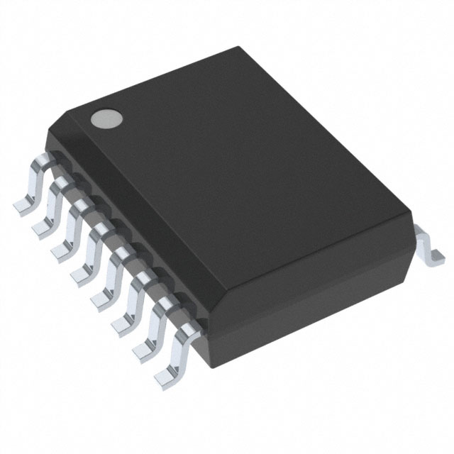
ISO6742FQDWRQ1

Why Choose Us?
Professional Platform
B2B & B2C purchasingDelivery at full speed
1-2 days deliveryWide variety
Original manufacturers365 days guarantee
Responsible quality
.png)


Tech Specifications
ISO6742FQDWRQ1 Description
The Texas Instruments ISO6742FQDWRQ1 is a highly integrated single-chip solution designed for automotive applications. It is a precision voltage and current sensing device that provides high accuracy and low power consumption. Here is a description of the model, its features, and potential applications:
Description:
The ISO6742FQDWRQ1 is a member of Texas Instruments' automotive-grade isolated amplifiers and drivers family. It is designed to meet the stringent requirements of automotive applications, offering robust performance, high precision, and reliable operation in harsh environments.
Features:
-
Automotive Grade: The device is designed to meet the stringent requirements of automotive applications, including temperature ranges, vibration, and shock resistance.
-
Isolated Amplifier: It provides galvanic isolation between the input and output, which is crucial for safety and noise immunity in automotive systems.
-
Precision Sensing: The device offers high precision in voltage and current sensing, which is essential for accurate monitoring and control of automotive systems.
-
Low Power Consumption: It is designed for low power operation, which is important for battery-powered systems and to reduce the overall energy consumption of the vehicle.
-
Wide Input Voltage Range: The device can operate with a wide range of input voltages, making it suitable for various automotive systems with different power supply requirements.
-
Small Package Size: The ISO6742FQDWRQ1 is available in a compact package, which is beneficial for space-constrained automotive applications.
-
Robust Performance: It is designed to operate reliably in harsh automotive environments, with features like over-voltage protection, under-voltage lockout, and thermal shutdown.
Applications:
-
Battery Management Systems (BMS): The device can be used for accurate voltage and current monitoring in electric and hybrid vehicles' battery packs.
-
Motor Control: It can be used for precise current sensing in electric motor drive systems, which is crucial for efficient and reliable operation.
-
Power Management: The ISO6742FQDWRQ1 can be used for monitoring and controlling power distribution in automotive systems, such as powertrain control modules and energy management systems.
-
Charging Systems: It can be used in electric vehicle charging systems for accurate current and voltage sensing, ensuring safe and efficient charging.
-
Sensor Interfaces: The device can be used as an interface for various types of sensors in automotive applications, providing isolation and signal conditioning.
-
In-Vehicle Networks: It can be used in in-vehicle communication networks for reliable data transmission between different electronic control units (ECUs).
In summary, the Texas Instruments ISO6742FQDWRQ1 is a versatile and high-performance device designed for demanding automotive applications, offering precision sensing, isolation, and low power consumption in a compact package.
FAQ
Not available to buy online? Want the lower wholesale price? Please Send RFQ to get best price, we will respond immediately


.png?x-oss-process=image/format,webp/resize,h_32)


