
Texas Instruments
JM38510/30103B2A
Flip Flops


.png?x-oss-process=image/format,webp/resize,p_30)


JM38510/30103B2A Description
JM38510/30103B2A Description
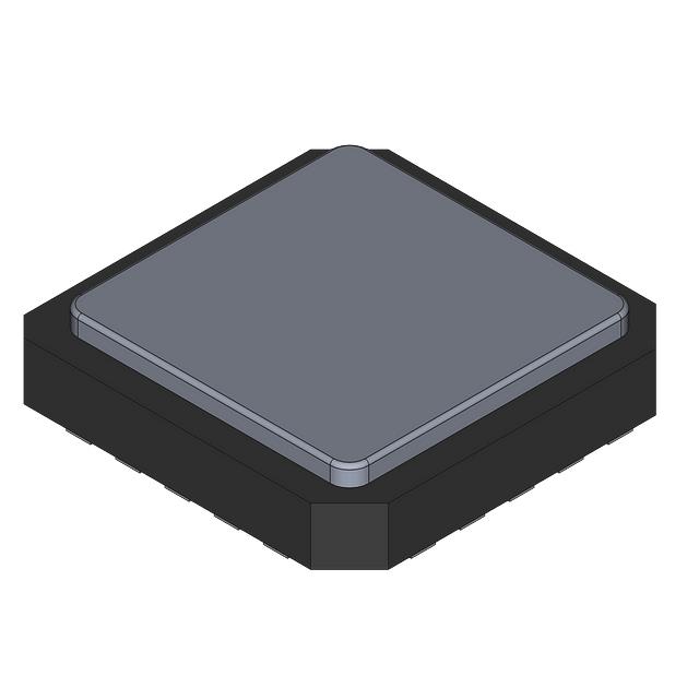
The JM38510/30103B2A is a high-performance Logic IC Chip manufactured by Texas Instruments, a leading innovator in semiconductor technology. This dual J-K negative-edge-triggered flip-flop is designed to provide reliable and efficient performance in various digital circuits. The device is categorized under the Logic IC Chips and is currently in an active product status, ensuring continued availability and support for existing and future applications.
JM38510/30103B2A Features
The JM38510/30103B2A is engineered with several key features that make it a standout choice for digital logic applications:
- Dual J-K Flip-Flops: The device integrates two independent J-K flip-flops, each capable of being triggered on the negative edge of the clock signal. This dual functionality allows for efficient use of space and resources in complex digital circuits.
- Negative-Edge Triggering: The negative-edge triggering mechanism ensures precise timing control, making it ideal for applications requiring accurate synchronization.
- Low Power Consumption: The 54LS112A series is known for its low power consumption, which is crucial for battery-operated devices and systems where energy efficiency is paramount.
- High-Speed Operation: The device operates at high speeds, ensuring rapid data processing and minimal latency, which is essential for high-performance digital systems.
- Bulk Packaging: Available in bulk packaging, the JM38510/30103B2A is suitable for large-scale production and integration into various electronic assemblies.
- Compliance and Standards: The product adheres to the ECCN classification of EAR99 and falls under the HTSUS code 8542.39.0001, ensuring compliance with international trade regulations.
JM38510/30103B2A Applications
The JM38510/30103B2A is versatile and finds application in a wide range of electronic systems:
- Digital Clocks and Timers: The precise negative-edge triggering and dual functionality make it ideal for applications requiring accurate timekeeping and synchronization.
- Sequential Logic Circuits: The device is well-suited for use in sequential logic circuits, where the state of the output depends on the sequence of input signals.
- Data Storage and Retrieval Systems: The dual J-K flip-flops can be used to store and manage binary data efficiently, making it a valuable component in data storage and retrieval systems.
- Telecommunications: In communication systems, the high-speed operation and low power consumption of the JM38510/30103B2A make it suitable for signal processing and control functions.
- Consumer Electronics: The device's compact size and bulk packaging make it ideal for integration into consumer electronics, where space and cost efficiency are critical.
Conclusion of JM38510/30103B2A
The JM38510/30103B2A from Texas Instruments is a robust and versatile Logic IC Chip that offers significant advantages over similar models. Its dual J-K flip-flops, negative-edge triggering, low power consumption, and high-speed operation make it a reliable choice for a variety of digital logic applications. Whether used in digital clocks, sequential logic circuits, or data storage systems, the JM38510/30103B2A ensures efficient performance and compliance with international standards. For engineers and designers seeking a high-quality, reliable, and efficient logic IC solution, the JM38510/30103B2A is an excellent choice.
Tech Specifications
JM38510/30103B2A Documents
Download datasheets and manufacturer documentation for JM38510/30103B2A
Shopping Guide


.png?x-oss-process=image/format,webp/resize,h_32)


