
Texas Instruments
JM38510/30107B2A
Flip Flops


.png?x-oss-process=image/format,webp/resize,p_30)


JM38510/30107B2A Description
JM38510/30107B2A Description
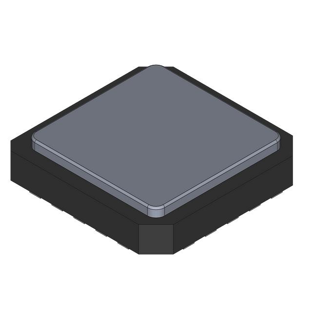
The JM38510/30107B2A is a high-performance, quadruple D-type flip-flop designed for a wide range of digital applications. Manufactured by Texas Instruments, this logic IC chip is part of the 54LS series, known for its reliability and efficiency. The device operates within a supply voltage range of 4.5V to 5.5V and features a clock frequency of 40 MHz, ensuring fast and accurate data processing. With a maximum propagation delay of 25ns at 5V and 15pF, the JM38510/30107B2A delivers exceptional performance in high-speed digital circuits.
JM38510/30107B2A Features
- Clock Frequency: 40 MHz, enabling high-speed operation suitable for demanding digital applications.
- Max Propagation Delay: 25ns @ 5V, 15pF, ensuring minimal delay in signal transmission.
- Current - Quiescent (Iq): 18 mA, providing low power consumption during idle states.
- Number of Bits per Element: 4, supporting multiple data storage and processing tasks.
- Output Type: Complementary, offering flexibility in circuit design.
- Trigger Type: Positive Edge, ensuring reliable data capture on the rising edge of the clock signal.
- Mounting Type: Surface Mount, facilitating compact and efficient PCB layouts.
- Product Status: Active, ensuring continued availability and support.
- Series: 54LS, known for its robustness and compatibility with a wide range of digital systems.
- Function: Master Reset, providing a reliable means to reset the flip-flops to a known state.
- Voltage - Supply: 4.5V ~ 5.5V, offering flexibility in power supply requirements.
- Mfr: Texas Instruments, a leading manufacturer known for quality and innovation.
- Number of Elements: 1, ensuring simplicity and ease of integration.
- Package: Tube, providing protection and ease of handling during manufacturing.
- RoHS Status: ROHS3 Compliant, ensuring environmental sustainability.
- Current - Output High, Low: 400µA, 4mA, providing robust output drive capabilities.
- Moisture Sensitivity Level (MSL): Not Applicable, reducing concerns about moisture-related issues.
JM38510/30107B2A Applications
The JM38510/30107B2A is ideal for a variety of applications where high-speed data processing and reliable performance are critical. Its quadruple D-type flip-flop design makes it suitable for digital signal processing, data storage, and control systems. Specific use cases include:
- Digital Signal Processing: Efficiently handling high-speed data in communication systems and digital filters.
- Data Storage: Storing and processing multiple bits of data in memory circuits.
- Control Systems: Implementing state machines and control logic in industrial automation and robotics.
- Clock Management: Managing clock signals in complex digital circuits to ensure synchronous operation.
- Consumer Electronics: Enhancing the performance of digital devices such as smartphones, tablets, and gaming consoles.
Conclusion of JM38510/30107B2A
The JM38510/30107B2A stands out as a versatile and high-performance logic IC chip, offering significant advantages over similar models. Its combination of high clock frequency, low propagation delay, and robust output capabilities make it an ideal choice for demanding digital applications. The device's compliance with ROHS3 standards and its surface mount packaging further enhance its appeal for modern electronics manufacturing. Whether used in digital signal processing, data storage, or control systems, the JM38510/30107B2A delivers reliable performance and ease of integration, making it a valuable component in the electronics industry.
Tech Specifications
JM38510/30107B2A Documents
Download datasheets and manufacturer documentation for JM38510/30107B2A
 Datasheet
 Shopping Guide


.png?x-oss-process=image/format,webp/resize,h_32)


