
 German
 Japanese
 Portuguese
 Korea
Korea
 Mexico
 Dutch
Dutch


Texas Instruments
JM38510/30301SDA

Why Choose Us?
Professional Platform
B2B & B2C purchasingDelivery at full speed
1-2 days deliveryWide variety
Original manufacturers365 days guarantee
Responsible quality
.png)


Tech Specifications
JM38510/30301SDA Description
JM38510/30301SDA Description
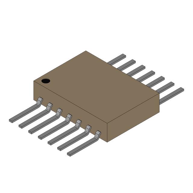
The JM38510/30301SDA is a high-performance NOR gate logic IC chip manufactured by Texas Instruments, designed for a wide range of digital applications. This device belongs to the 54LS02 series and is housed in a 14-pin ceramic flat pack (CFP) package. It features four independent NOR gates, each with two inputs, making it highly versatile for various digital logic operations.
The IC operates within a supply voltage range of 4.5V to 5.5V, ensuring compatibility with standard 5V digital systems. It boasts a maximum propagation delay of 15 nanoseconds at 5V with a load capacitance of 15 picofarads, providing rapid signal processing capabilities. The input logic levels are specified as 0.7V for low and 2V for high, ensuring reliable operation with minimal voltage margins.
The JM38510/30301SDA is designed for surface mount applications, offering a compact and robust solution for modern electronic designs. It features a maximum quiescent current of 5.4 mA, with output currents of 400µA for high and 4mA for low, ensuring efficient power usage and reliable signal integrity.
JM38510/30301SDA Features
- High-Speed Performance: With a maximum propagation delay of 15ns at 5V and 15pF, the JM38510/30301SDA ensures fast signal processing, making it ideal for high-speed digital circuits.
- Versatile Logic Function: The NOR gate logic type provides a fundamental building block for digital logic design, enabling the creation of complex digital systems.
- Wide Operating Voltage Range: The 4.5V to 5.5V supply voltage range offers flexibility and compatibility with standard 5V digital systems.
- Low Power Consumption: The maximum quiescent current of 5.4 mA and output currents of 400µA (high) and 4mA (low) ensure efficient power usage, making it suitable for power-sensitive applications.
- Surface Mount Compatibility: The surface mount design allows for easy integration into modern PCB designs, enhancing reliability and reducing the overall footprint.
- ROHS3 Compliant: The JM38510/30301SDA meets the stringent environmental standards of ROHS3, ensuring compliance with global regulations and promoting sustainable manufacturing practices.
JM38510/30301SDA Applications
The JM38510/30301SDA is well-suited for a variety of applications due to its high-speed performance, low power consumption, and versatile logic function. Some specific use cases include:
- Digital Logic Circuits: Ideal for constructing digital logic systems, such as decoders, multiplexers, and other combinational logic circuits.
- Microcontroller Peripherals: Enhances the functionality of microcontrollers by providing additional logic processing capabilities.
- Communication Systems: Utilized in digital communication systems for signal processing and control logic.
- Consumer Electronics: Integrated into consumer electronics for various digital logic operations, ensuring reliable and efficient performance.
- Industrial Control Systems: Employed in industrial control systems for signal processing and control logic, contributing to the overall efficiency and reliability of the system.
Conclusion of JM38510/30301SDA
The JM38510/30301SDA is a high-performance NOR gate logic IC chip that offers a combination of speed, versatility, and efficiency. Its low propagation delay, wide operating voltage range, and low power consumption make it an ideal choice for a variety of digital applications. The surface mount design and ROHS3 compliance further enhance its suitability for modern electronic designs. Whether used in digital logic circuits, microcontroller peripherals, or industrial control systems, the JM38510/30301SDA delivers reliable performance and robust functionality, making it a valuable component in the electronics industry.
FAQ
| Quantity | Unit Price | Ext. Price |
|---|---|---|
| 1+ | $234.30880 | $234.31 |
Not available to buy online? Want the lower wholesale price? Please Send RFQ to get best price, we will respond immediately


.png?x-oss-process=image/format,webp/resize,h_32)


