
 German
 Japanese
 Portuguese
 Korea
Korea
 Mexico
 Dutch
Dutch


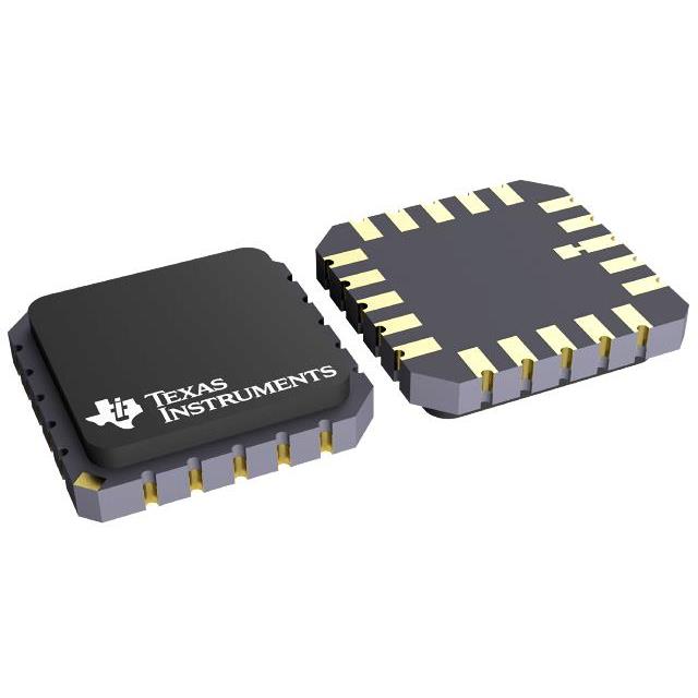


Texas Instruments
JM38510/32503BSA

Why Choose Us?
Professional Platform
B2B & B2C purchasingDelivery at full speed
1-2 days deliveryWide variety
Original manufacturers365 days guarantee
Responsible quality
.png)


Tech Specifications
JM38510/32503BSA Description
JM38510/32503BSA Description
The JM38510/32503BSA is a high-performance 54LS374 Octal D-Type Edge Trigger Flip-Flop manufactured by Texas Instruments. This device is designed to provide reliable and efficient data storage and transfer capabilities, making it an essential component in various digital systems. The 54LS374 is part of the 54LS series, known for its low power consumption and high-speed performance.
The JM38510/32503BSA features an Octal D-Type Edge Trigger Flip-Flop configuration, which allows it to store eight bits of data. This configuration ensures that data is captured on the rising edge of the clock signal, providing precise and synchronized data handling. The device operates within a wide range of supplyages volt, ensuring compatibility with various digital systems.
JM38510/32503BSA Features
- Octal D-Type Edge Trigger Flip-Flop: The JM38510/32503BSA is designed with an octal configuration, enabling it to handle eight bits of data simultaneously. This feature is particularly beneficial in applications requiring high data throughput and efficient data storage.
- Low Power Consumption: As part of the 54LS series, this device offers low power consumption, making it suitable for battery-operated and energy-efficient systems.
- High-Speed Performance: The 54LS374 is known for its high-speed operation, ensuring fast data transfer and minimal latency in digital circuits.
- Edge Triggering: The device captures data on the rising edge of the clock signal, providing precise timing and synchronization.
- Bulk Packaging: The JM38510/32503BSA is available in bulk packaging, which is ideal for large-scale production and inventory management.
- Active Product Status: This product is currently active, ensuring availability and support from Texas Instruments.
JM38510/32503BSA Applications
The JM38510/32503BSA is ideal for a variety of applications due to its high-speed performance and low power consumption. Some specific use cases include:
- Data Latching: The device is commonly used in data latching applications where it captures and holds data until it is needed for further processing.
- Memory Buffers: It serves as an efficient memory buffer in systems requiring temporary data storage and transfer.
- Digital Systems: The JM38510/32503BSA is suitable for use in various digital systems, including microprocessors, microcontrollers, and digital signal processors.
- Telecommunications: In telecommunication systems, it can be used for data synchronization and buffering.
- Consumer Electronics: The device is also used in consumer electronics, such as digital cameras and video game consoles, where reliable data handling is crucial.
Conclusion of JM38510/32503BSA
The JM38510/32503BSA from Texas Instruments is a robust and versatile Octal D-Type Edge Trigger Flip-Flop that offers significant advantages over similar models. Its low power consumption, high-speed performance, and precise edge triggering make it an ideal choice for a wide range of digital applications. Whether used in data latching, memory buffering, or digital systems, the JM38510/32503BSA ensures reliable and efficient data handling. With its active product status and bulk packaging, it is a reliable and cost-effective solution for both small-scale projects and large-scale production.
FAQ
| Quantity | Unit Price | Ext. Price |
|---|---|---|
| 6+ | $42.07280 | $252.44 |
Not available to buy online? Want the lower wholesale price? Please Send RFQ to get best price, we will respond immediately


.png?x-oss-process=image/format,webp/resize,h_32)


