

Texas Instruments
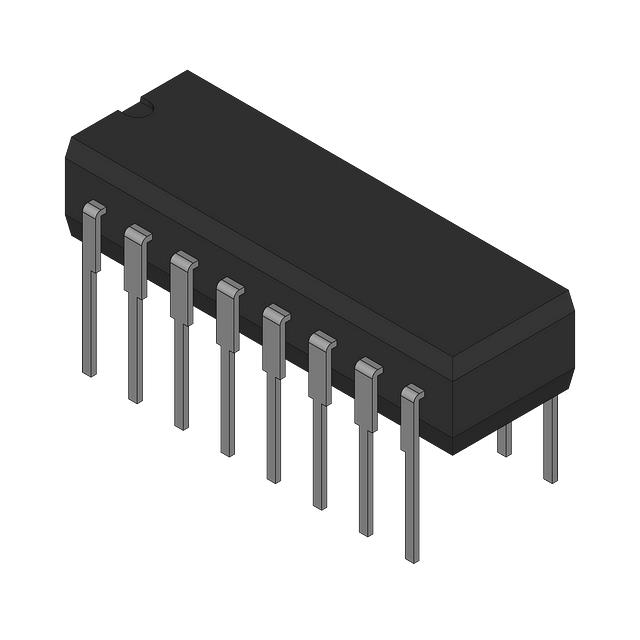
JM38510/37102BEA
Flip Flops

Not available to buy online? Want the lower wholesale price? Please Send RFQ to get best price, we will respond immediately


.png?x-oss-process=image/format,webp/resize,p_30)


JM38510/37102BEA Description
JM38510/37102BEA Description
The JM38510/37102BEA is a dual J-K positive-edge-triggered flip-flop from Texas Instruments, designed for high-performance applications requiring precise control and reliable operation. This logic IC chip belongs to the 54ALS series and is optimized for use in a wide range of digital systems. The device features a clock frequency of 30 MHz, ensuring fast and efficient data processing. It operates within a supply voltage range of 4.5V to 5.5V, making it suitable for various power supply configurations.
The JM38510/37102BEA offers a maximum propagation delay of 21ns at 5V and 50pF, which is crucial for maintaining signal integrity and minimizing latency in high-speed digital circuits. The flip-flop is designed with a quiescent current of 4 mA, which helps in reducing power consumption, making it ideal for energy-efficient designs. Each flip-flop element consists of a single bit and supports complementary outputs, providing flexibility in circuit design.
The device is triggered on the positive edge, ensuring precise timing control and synchronization with other digital components. It features set (preset) and reset functions, which allow for easy initialization and control of the flip-flop states. The output current capabilities are 400µA for high and 4mA for low, ensuring robust signal drive and compatibility with a variety of load conditions.
The JM38510/37102BEA is packaged in a through-hole format, making it suitable for traditional PCB assembly methods. The device is compliant with ROHS3 standards, ensuring environmental sustainability and adherence to regulatory requirements. Additionally, the moisture sensitivity level (MSL) is not applicable, making it suitable for a wide range of operating environments.
JM38510/37102BEA Features
- High Clock Frequency: Operates at a clock frequency of 30 MHz, enabling high-speed data processing and synchronization.
- Low Propagation Delay: Achieves a maximum propagation delay of 21ns at 5V and 50pF, ensuring minimal latency and precise timing control.
- Low Quiescent Current: Consumes only 4 mA in quiescent state, contributing to energy-efficient designs.
- Complementary Outputs: Provides complementary outputs for each flip-flop element, offering flexibility in circuit design.
- Positive-Edge Triggering: Ensures reliable and precise timing control by triggering on the positive edge of the clock signal.
- Set and Reset Functions: Includes set (preset) and reset capabilities, allowing for easy initialization and control of flip-flop states.
- Robust Output Current: Delivers 400µA for high and 4mA for low output currents, ensuring strong signal drive and compatibility with various load conditions.
- Through-Hole Mounting: Suitable for traditional PCB assembly methods, providing ease of integration into existing systems.
- ROHS3 Compliant: Adheres to environmental sustainability standards, ensuring compliance with regulatory requirements.
JM38510/37102BEA Applications
The JM38510/37102BEA is ideal for a variety of applications where precise timing control and reliable operation are critical. Some specific use cases include:
- Digital Clock Circuits: Utilized in clock generation and synchronization circuits where high-speed and low-latency performance are essential.
- Sequential Logic Systems: Employed in sequential logic systems requiring precise control and state management, such as counters and state machines.
- Data Processing Units: Integrated into data processing units where reliable and fast flip-flop operation is necessary for data integrity and processing speed.
- Communication Systems: Used in communication systems for signal synchronization and data transmission control.
- Control Systems: Applied in control systems for precise timing and state control, ensuring reliable operation and system stability.
Conclusion of JM38510/37102BEA
The JM38510/37102BEA from Texas Instruments stands out as a high-performance dual J-K positive-edge-triggered flip-flop, offering a combination of speed, precision, and reliability. Its low propagation delay, low quiescent current, and robust output current capabilities make it an excellent choice for high-speed digital systems. The inclusion of set and reset functions, along with complementary outputs, provides additional flexibility and control in circuit design.
The device's compliance with ROHS3 standards and its through-hole mounting format ensure ease of integration and environmental sustainability. Whether used in digital clock circuits, sequential logic systems, or data processing units, the JM38510/37102BEA delivers exceptional performance and reliability, making it a preferred choice for engineers and designers in the electronics industry.
Tech Specifications
JM38510/37102BEA Documents
Download datasheets and manufacturer documentation for JM38510/37102BEA
Related Parts


Shopping Guide


.png?x-oss-process=image/format,webp/resize,h_32)


©2025 ERSA Electronics Corporation.