
Texas Instruments
JM38510/65302BCA
Flip Flops


.png?x-oss-process=image/format,webp/resize,p_30)


JM38510/65302BCA Description
JM38510/65302BCA Description
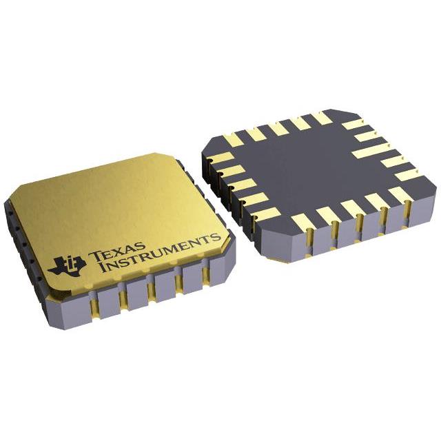
The JM38510/65302BCA is a dual D-type positive-edge-triggered flip-flop from Texas Instruments, designed for high-performance digital logic applications. This device is part of the 54HC series, known for its robustness and reliability in various electronic systems. The IC operates within a supply voltage range of 2V to 6V, making it versatile for different power supply configurations. It features a clock frequency of 60 MHz, ensuring fast and efficient data processing.
The JM38510/65302BCA offers a maximum propagation delay of 30ns at 6V and 50pF, which is crucial for high-speed applications where timing precision is essential. It consumes a quiescent current of only 4 µA, making it energy-efficient and suitable for low-power designs. Each flip-flop element supports one bit of data, with complementary outputs that provide flexibility in circuit design. The device is triggered on the positive edge of the clock signal, ensuring reliable data latching.
Packaged in a tube, this through-hole mounted IC is ideal for applications requiring robust mechanical stability. It complies with ROHS3 standards, ensuring environmental sustainability and regulatory compliance. The input capacitance is 3 pF, and the output current capability is 5.2mA for both high and low states, providing robust drive capabilities for downstream circuits.
JM38510/65302BCA Features
- High-Speed Operation: With a clock frequency of 60 MHz, the JM38510/65302BCA ensures rapid data processing, making it suitable for high-speed digital systems.
- Low Propagation Delay: The maximum propagation delay of 30ns at 6V and 50pF ensures precise timing control, critical for synchronous operations.
- Low Power Consumption: The quiescent current of 4 µA makes this IC highly energy-efficient, ideal for battery-powered and low-power applications.
- Versatile Supply Voltage: Operating within a 2V to 6V supply voltage range, it offers flexibility in power supply design.
- Robust Output Capability: With 5.2mA output current for both high and low states, it can drive multiple downstream components effectively.
- Environmental Compliance: ROHS3 compliant, ensuring it meets the latest environmental standards and regulatory requirements.
- Mechanical Stability: Through-hole mounting and tube packaging provide robust mechanical stability, suitable for industrial and rugged environments.
JM38510/65302BCA Applications
The JM38510/65302BCA is ideal for a wide range of applications due to its high-speed operation, low power consumption, and robust performance. Some specific use cases include:
- Digital Clock Circuits: Its high-speed and precise timing capabilities make it suitable for generating and managing clock signals in digital systems.
- Data Latching: The positive-edge-triggered flip-flops are ideal for latching data in synchronous digital circuits, ensuring reliable data transfer.
- Frequency Dividers: The device can be used to create frequency dividers, reducing clock frequencies for various sub-systems within a larger digital circuit.
- Counter Circuits: It can be employed in counter circuits to count clock pulses, useful in timing and control applications.
- Memory Elements: The dual D-type flip-flops can serve as memory elements in digital logic circuits, storing data bits for processing and control functions.
Conclusion of JM38510/65302BCA
The JM38510/65302BCA from Texas Instruments is a high-performance dual D-type positive-edge-triggered flip-flop that offers a combination of speed, efficiency, and reliability. Its low propagation delay and high-speed operation make it ideal for applications requiring precise timing control. The low power consumption and wide supply voltage range provide flexibility in design, while its robust output capability ensures it can drive multiple components effectively.
With its compliance to ROHS3 standards and through-hole mounting, the JM38510/65302BCA is not only environmentally friendly but also mechanically stable, making it suitable for a variety of industrial and rugged applications. Whether used in digital clock circuits, data latching, frequency dividers, counter circuits, or as memory elements, the JM38510/65302BCA stands out as a versatile and reliable choice for digital logic applications.
Tech Specifications
JM38510/65302BCA Documents
Download datasheets and manufacturer documentation for JM38510/65302BCA
Shopping Guide


.png?x-oss-process=image/format,webp/resize,h_32)


