
 German
 Japanese
 Portuguese
 Korea
Korea
 Mexico
 Dutch
Dutch


Texas Instruments
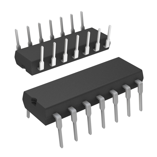
LF444CN/NOPB

Why Choose Us?
Professional Platform
B2B & B2C purchasingDelivery at full speed
1-2 days deliveryWide variety
Original manufacturers365 days guarantee
Responsible quality
.png)


Tech Specifications
LF444CN/NOPB Description
The LF444CN/NOPB is a low power, precision operational amplifier (op-amp) manufactured by Texas Instruments. It is designed for use in a wide range of applications where low power consumption and high precision are required.
Description:
The LF444CN/NOPB is a JFET input operational amplifier that offers high input impedance and low input offset voltage. It is available in an 8-pin DIP (dual in-line package) package. The device has a wide supply voltage range of ±2.5V to ±18V, which makes it suitable for use in a variety of power supply configurations.
Features:
- Low power consumption: The LF444CN/NOPB operates with a supply current of only 800µA, making it ideal for battery-powered applications.
- High input impedance: The JFET input stage provides high input impedance, which minimizes the loading effect on the input signal source.
- Low input offset voltage: The device has an input offset voltage of typically 1mV, which ensures high precision in applications that require accurate amplification of small signals.
- Wide supply voltage range: The LF444CN/NOPB can operate with supply voltages ranging from ±2.5V to ±18V, making it suitable for a wide range of applications.
- Low output noise: The device has a low output noise of 8nV/√Hz, which is beneficial for applications that require low noise amplification.
Applications:
The LF444CN/NOPB is suitable for a variety of applications where low power consumption and high precision are required. Some of the common applications include:
- Battery-powered instruments: The low power consumption of the LF444CN/NOPB makes it ideal for use in battery-powered instruments, such as portable medical devices and data acquisition systems.
- Strain gauge amplifiers: The high input impedance and low input offset voltage of the device make it suitable for use in strain gauge amplifiers, which require precise amplification of small signals.
- pH meter amplifiers: The LF444CN/NOPB can be used in pH meter amplifiers, where high precision and low drift are required.
- Pressure sensor amplifiers: The device can be used in pressure sensor amplifiers, where low noise and high precision are essential for accurate measurements.
- Audio amplifiers: The LF444CN/NOPB can be used in audio amplifiers, where low noise and low distortion are important for high-quality audio reproduction.
In summary, the LF444CN/NOPB is a low power, precision operational amplifier that offers high input impedance, low input offset voltage, and low output noise. It is suitable for a wide range of applications, including battery-powered instruments, strain gauge amplifiers, pH meter amplifiers, pressure sensor amplifiers, and audio amplifiers.
FAQ
Not available to buy online? Want the lower wholesale price? Please Send RFQ to get best price, we will respond immediately


.png?x-oss-process=image/format,webp/resize,h_32)


