
 German
 Japanese
 Portuguese
 Korea
Korea
 Mexico
 Dutch
Dutch


Texas Instruments
LM536005QDSXRQ1

Why Choose Us?
Professional Platform
B2B & B2C purchasingDelivery at full speed
1-2 days deliveryWide variety
Original manufacturers365 days guarantee
Responsible quality
.png)


Tech Specifications
LM536005QDSXRQ1 Description
The LM536005QDSXRQ1 is a high-performance, low-power, quad operational amplifier (op-amp) from Texas Instruments. This device is designed to provide excellent DC and AC performance in a small package, making it suitable for a wide range of applications.
Description:
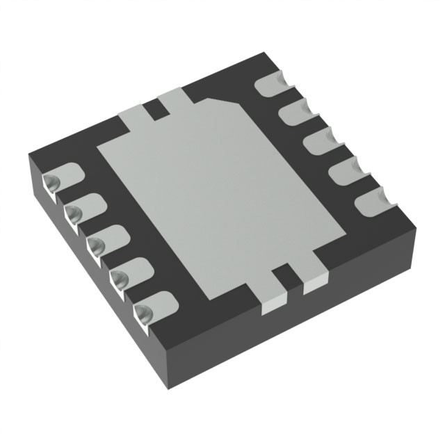
The LM536005QDSXRQ1 is a quad operational amplifier that features low input offset voltage, low input bias current, and low noise characteristics. It is available in a compact 10-lead QFN package, making it ideal for space-constrained applications.
Features:
- Low input offset voltage: The LM536005QDSXRQ1 has an input offset voltage as low as 1 mV, which makes it suitable for precision applications.
- Low input bias current: The input bias current is as low as 60 pA, which helps to minimize errors in high-impedance circuits.
- Low noise: The device has a low input voltage noise of 8.5 nV/√Hz, making it suitable for applications that require low-noise amplification.
- Wide supply voltage range: The LM536005QDSXRQ1 can operate from a supply voltage range of 2.7 V to 10.8 V, making it suitable for a wide range of applications.
- High output current: The device can sink or source up to 25 mA from each output, making it suitable for driving high-current loads.
- Short-circuit protection: The LM536005QDSXRQ1 features internal protection against output short circuits, which helps to prevent damage to the device.
Applications:
The LM536005QDSXRQ1 is suitable for a wide range of applications, including:
- Audio amplification: The low noise and low distortion characteristics of the LM536005QDSXRQ1 make it suitable for use in audio amplifiers.
- Strain gauge amplifiers: The low input offset voltage and low drift of the LM536005QDSXRQ1 make it ideal for use in strain gauge amplifiers.
- Medical instrumentation: The device's low noise and low input bias current characteristics make it suitable for use in medical instruments that require precise amplification.
- Industrial control systems: The LM536005QDSXRQ1 can be used in industrial control systems that require high output current and low noise amplification.
- Battery monitoring systems: The low supply voltage and low power consumption of the LM536005QDSXRQ1 make it suitable for use in battery monitoring systems.
In summary, the LM536005QDSXRQ1 is a high-performance, low-power, quad operational amplifier from Texas Instruments that offers excellent DC and AC performance in a small package. Its low input offset voltage, low input bias current, and low noise characteristics make it suitable for a wide range of applications, including audio amplification, strain gauge amplifiers, medical instrumentation, industrial control systems, and battery monitoring systems.
FAQ
| Quantity | Unit Price | Ext. Price |
|---|---|---|
| 1+ | $6.19200 | $6.19 |
| 10+ | $6.04628 | $60.46 |
| 30+ | $5.95028 | $178.51 |
Not available to buy online? Want the lower wholesale price? Please Send RFQ to get best price, we will respond immediately


.png?x-oss-process=image/format,webp/resize,h_32)


