
Texas Instruments
LMC6035IM/NOPB
OP Amps, Buffer Amps ICs


.png?x-oss-process=image/format,webp/resize,p_30)


LMC6035IM/NOPB Description
LMC6035IM/NOPB Description
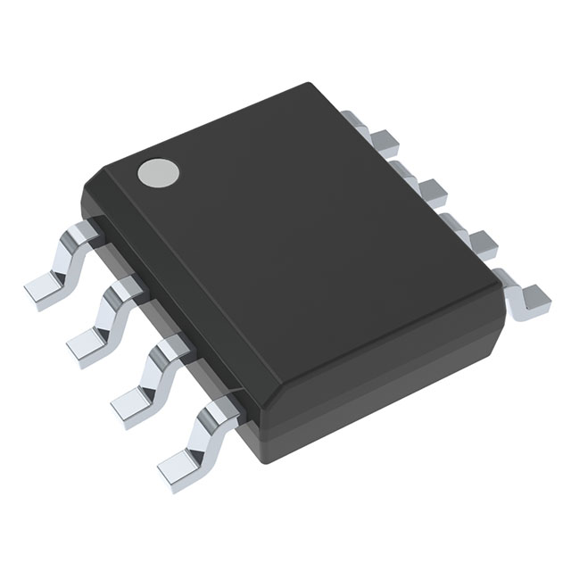
The LMC6035IM/NOPB is a dual CMOS operational amplifier designed by Texas Instruments, featuring a wide supply voltage range from 2 V to 15.5 V. This IC is housed in an 8SOIC package, making it suitable for surface-mount applications. Despite its obsolescence, the LMC6035IM/NOPB remains a robust choice for various linear amplifier applications due to its unique combination of low input bias current, high slew rate, and compliance with industry standards such as REACH and RoHS3.
LMC6035IM/NOPB Features
- Wide Supply Voltage Range: Operates from 2 V to 15.5 V, providing in flexibility power supply requirements.
- Low Input Bias Current: At just 0.02 pA, this feature minimizes the impact of input current on the overall circuit performance, making it ideal for high-impedance applications.
- High Slew Rate: A 1.5 V/µs slew rate ensures fast response times, crucial for applications requiring rapid signal processing.
- Gain Bandwidth Product: With a gain bandwidth product of 1.4 MHz, the LMC6035IM/NOPB can handle a wide range of frequencies while maintaining signal integrity.
- Low Input Offset Voltage: An input offset voltage of 500 µV ensures accurate signal amplification with minimal distortion.
- Dual Channel Design: Each channel can source or sink up to 8 mA of current, providing ample drive capability for various loads.
- Compliance and Reliability: The LMC6035IM/NOPB is REACH unaffected and RoHS3 compliant, ensuring it meets environmental and safety standards. Additionally, its moisture sensitivity level is 1 (unlimited), making it suitable for a wide range of environmental conditions.
LMC6035IM/NOPB Applications
The LMC6035IM/NOPB is well-suited for applications that require high precision and low noise, such as:
- Precision Signal Conditioning: Ideal for amplifying and conditioning low-level signals in sensors and transducers.
- High-Impedance Applications: Its low input bias current makes it suitable for applications involving high-impedance sources, such as photodiodes and pH probes.
- Analog Signal Processing: The wide supply voltage range and high slew rate make it suitable for analog signal processing in various electronic systems.
- Medical and Industrial Equipment: The combination of low input offset voltage and high slew rate ensures accurate and reliable performance in medical and industrial applications.
Conclusion of LMC6035IM/NOPB
The LMC6035IM/NOPB, despite being obsolete, remains a valuable component in the electronics industry due to its unique features and performance benefits. Its wide supply voltage range, low input bias current, and high slew rate make it an excellent choice for applications requiring precision and reliability. While newer models may offer additional features, the LMC6035IM/NOPB continues to provide a reliable and cost-effective solution for various linear amplifier applications.
Tech Specifications
LMC6035IM/NOPB Documents
Download datasheets and manufacturer documentation for LMC6035IM/NOPB
 Mult Devices Wafer Fab Site 09/Mar/2017
  LMC6035/36
  Mult Dev EOL 7/Sep/2023
  LMC6035/36
  Mold Compound 24/Mar/2016
 Shopping Guide


.png?x-oss-process=image/format,webp/resize,h_32)


