
 German
 Japanese
 Portuguese
 Korea
Korea
 Mexico
 Dutch
Dutch


Texas Instruments
LMC6482IMMX

Why Choose Us?
Professional Platform
B2B & B2C purchasingDelivery at full speed
1-2 days deliveryWide variety
Original manufacturers365 days guarantee
Responsible quality
.png)


Tech Specifications
LMC6482IMMX Description
LMC6482IMMX Description
The LMC6482IMMX is a high-performance CMOS operational amplifier from Texas Instruments, designed to meet the demanding requirements of modern electronic systems. This dual-channel amplifier offers a wide supply voltage range, from a minimum of 3 V to a maximum of 15.5 V, making it suitable for a variety of power supply configurations. The LMC6482IMMX features a gain bandwidth product of 1.5 MHz, ensuring high-frequency performance and stability in signal processing applications. Its low input bias current of 0.02 pA minimizes offset errors, making it ideal for precision measurements and high-impedance circuits.
LMC6482IMMX Features
- Amplifier Type: CMOS
- Supply Voltage Range: 3 V to 15.5 V
- Gain Bandwidth Product: 1.5 MHz
- Input Bias Current: 0.02 pA
- Input Offset Voltage: 110 µV
- Slew Rate: 1.3 V/µs
- Supply Current: 1.3 mA per channel (for dual channels)
- Output Current per Channel: 30 mA
- Number of Circuits: 2
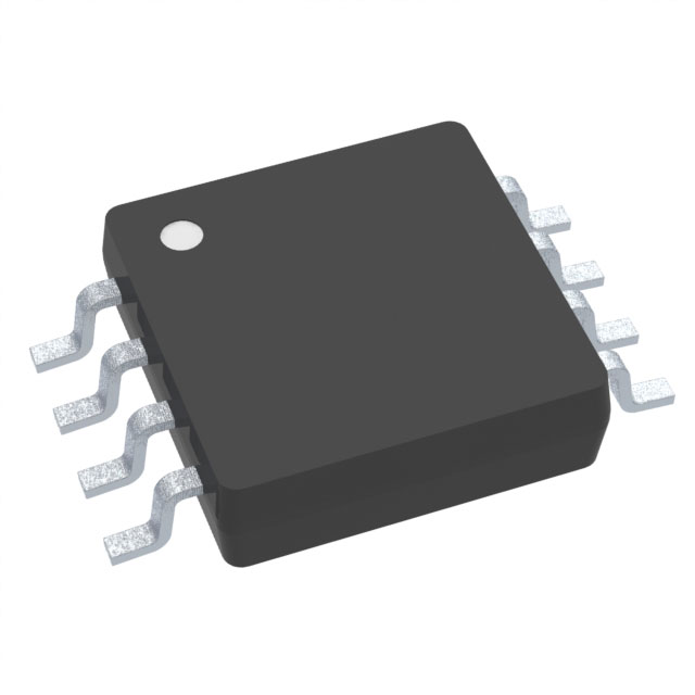
- Package Type: 8-VSSOP
- Mounting Type: Surface Mount
- Moisture Sensitivity Level (MSL): 1 (Unlimited)
- Compliance: REACH Unaffected, ROHS3 Compliant
- ECCN: EAR99
- HTSUS: 8542.33.0001
LMC6482IMMX Applications
The LMC6482IMMX is well-suited for a range of applications where precision and low power consumption are critical. Its low input bias current and input offset voltage make it ideal for high-impedance sensor interfaces and precision signal conditioning. The dual-channel design allows for compact and efficient circuit designs, reducing board space and component count. The wide supply voltage range and high slew rate ensure robust performance across various operating conditions.
Specific use cases include:
- Precision Signal Conditioning: Ideal for interfacing with high-impedance sensors, such as photodiodes and thermocouples, where minimal loading effects are crucial.
- Low-Power Systems: Suitable for battery-powered devices and portable electronics due to its low supply current.
- High-Frequency Applications: The 1.5 MHz gain bandwidth product and 1.3 V/µs slew rate make it suitable for applications requiring high-speed signal processing.
- Analog Signal Processing: Ideal for applications such as audio processing, where low distortion and high fidelity are required.
Conclusion of LMC6482IMMX
The LMC6482IMMX from Texas Instruments is a versatile and high-performance CMOS operational amplifier that offers a unique combination of low input bias current, low input offset voltage, and wide supply voltage range. Its dual-channel design and surface-mount package make it an excellent choice for compact and efficient circuit designs. The LMC6482IMMX is particularly well-suited for precision signal conditioning, low-power systems, and high-frequency applications. Its compliance with industry standards such as REACH and ROHS3 ensures that it meets the and environmental regulatory requirements of modern electronics manufacturing.
FAQ
Not available to buy online? Want the lower wholesale price? Please Send RFQ to get best price, we will respond immediately


.png?x-oss-process=image/format,webp/resize,h_32)


