
Texas Instruments
LMC6492BEM/NOPB
OP Amps, Buffer Amps ICs


.png?x-oss-process=image/format,webp/resize,p_30)


LMC6492BEM/NOPB Description
LMC6492BEM/NOPB Description
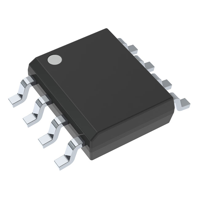
The LMC6492BEM/NOPB is a high-performance CMOS operational amplifier designed by Texas Instruments, featuring dual circuits in an 8SOIC package. This device is optimized for low power consumption and high precision, making it suitable for a wide range of applications. The LMC6492BEM/NOPB operates with a supply voltage range of 2.5 V to 15.5 V, ensuring flexibility in various power supply environments. It offers a gain bandwidth product of 1.5 MHz, which is ideal for applications requiring moderate speed and high accuracy. The amplifier's input bias current is extremely low at 0.15 pA, minimizing the impact on sensitive input signals. Additionally, the device has a low input offset voltage of 110 µV, ensuring high accuracy in signal processing.
LMC6492BEM/NOPB Features
- Low Power Consumption: The LMC6492BEM/NOPB consumes only 1.3 mA per channel, making it highly energy-efficient. This feature is particularly beneficial for battery-powered devices and portable applications where power conservation is critical.
- High Precision: With an input bias current of 0.15 pA and an input offset voltage of 110 µV, the LMC6492BEM/NOPB ensures high accuracy and minimal signal distortion. These characteristics are essential for precision instrumentation and measurement applications.
- Wide Operating Voltage Range: The device operates within a supply voltage range of 2.5 V to 15.5 V, providing flexibility and compatibility with various power supply systems.
- High Slew Rate: The LMC6492BEM/NOPB has a slew rate of 1.3 V/µs, which allows it to handle fast-changing signals effectively. This feature is crucial for applications requiring quick response times.
- Dual Circuits: The dual-channel design of the LMC6492BEM/NOPB enables the integration of multiple signal processing paths within a single package, reducing board space and component count.
- Surface Mount Technology: The surface mount package type facilitates easy integration into modern PCB designs and supports automated assembly processes.
LMC6492BEM/NOPB Applications
The LMC6492BEM/NOPB is well-suited for a variety of applications due to its combination of low power consumption, high precision, and wide operating voltage range. Some specific use cases include:
- Precision Signal Conditioning: Ideal for applications requiring accurate amplification and conditioning of low-level signals, such as in medical equipment, scientific instruments, and industrial sensors.
- Battery-Powered Devices: The low power consumption makes it suitable for portable devices and battery-operated systems where energy efficiency is paramount.
- Analog Signal Processing: The high slew rate and moderate gain bandwidth product make it suitable for applications involving analog signal processing, such as audio equipment and data acquisition systems.
- Automotive Electronics: The wide operating voltage range and robust performance ensure reliable operation in the varying voltage environments typical of automotive applications.
Conclusion of LMC6492BEM/NOPB
The LMC6492BEM/NOPB from Texas Instruments is a versatile CMOS operational amplifier that offers a balance of high precision, low power consumption, and wide operating voltage range. Its dual-channel design and surface mount package make it an excellent choice for a variety of applications, from precision instrumentation to portable devices. The low input bias current and input offset voltage ensure high accuracy and minimal signal distortion, while the high slew rate allows for effective handling of fast-changing signals. With its robust performance and flexibility, the LMC6492BEM/NOPB stands out as a reliable solution for modern electronic designs.
Tech Specifications
LMC6492BEM/NOPB Documents
Download datasheets and manufacturer documentation for LMC6492BEM/NOPB
 Mult Devices Wafer Fab Site 09/Mar/2017
  LMC6492AEMx/NOPB Datasheet
  OBS NOTICE 24/Oct/2023
 Shopping Guide


.png?x-oss-process=image/format,webp/resize,h_32)


