
 German
 Japanese
 Portuguese
 Korea
Korea
 Mexico
 Dutch
Dutch


Texas Instruments
LMC662AIN/NOPB

Why Choose Us?
Professional Platform
B2B & B2C purchasingDelivery at full speed
1-2 days deliveryWide variety
Original manufacturers365 days guarantee
Responsible quality
.png)


Tech Specifications
LMC662AIN/NOPB Description
LMC662AIN/NOPB Description
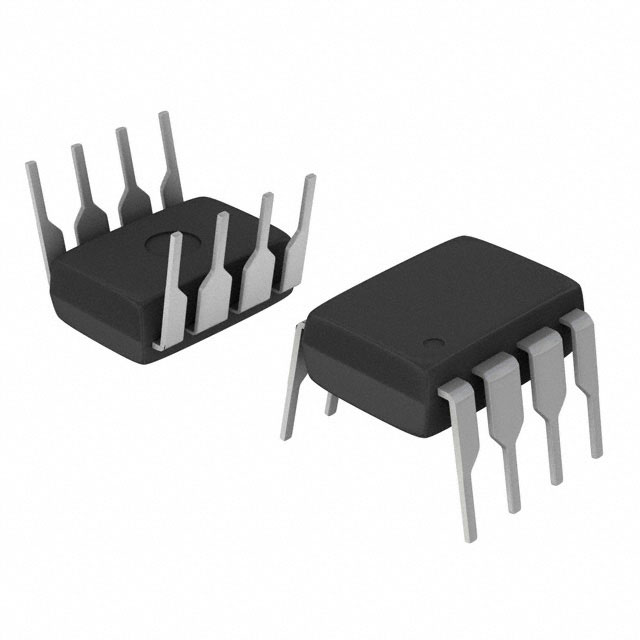
The LMC662AIN/NOPB is a dual CMOS operational amplifier from Texas Instruments, designed for a wide range of linear applications. This device features a supply voltage range from 4.75 V to 15.5 V, making it suitable for both low and high-voltage systems. With a gain bandwidth product of 1.4 MHz and a slew rate of 1.1 V/µs, the LMC662AIN/NOPB offers a balance between speed and power efficiency. Its low input bias current of 0.002 pA and input offset voltage of 1 mV ensure high precision and stability in signal processing. The device is housed in an 8-pin DIP package, ideal for through-hole mounting, and is available in a tube package format. The LMC662AIN/NOPB is RoHS3 compliant and unaffected by REACH regulations, ensuring compliance with environmental standards. With a moisture sensitivity level (MSL) of 1, it is suitable for unlimited storage conditions. This operational amplifier is part of the LMC® series and features two independent circuits, each capable of sourcing or sinking up to 40 mA of current.
LMC662AIN/NOPB Features
- Wide Supply Voltage Range: Operates from 4.75 V to 15.5 V, providing flexibility for various power supply configurations.
- High Gain Bandwidth Product: 1.4 MHz ensures stable performance across a broad frequency spectrum, making it suitable for high-frequency applications.
- Low Input Bias Current: 0.002 pA minimizes the impact on sensitive input signals, ideal for high-impedance sources.
- Low Input Offset Voltage: 1 mV ensures accurate signal processing and minimal error in precision applications.
- High Slew Rate: 1.1 V/µs allows for fast response times, crucial for applications requiring rapid signal changes.
- Dual Amplifier Configuration: Two independent circuits in a single package, reducing board space and component count.
- High Output Current: Each channel can source or sink up to 40 mA, suitable for driving various loads.
- Environmental Compliance: RoHS3 compliant and REACH unaffected, ensuring regulatory compliance.
- Moisture Sensitivity Level 1: Suitable for unlimited storage conditions, reducing handling and storage concerns.
- Through-Hole Mounting: Ideal for applications requiring robust mechanical stability and ease of assembly.
LMC662AIN/NOPB Applications
The LMC662AIN/NOPB is ideal for a variety of applications due to its versatile performance characteristics. Some specific use cases include:
- Signal Conditioning: Ideal for amplifying and conditioning low-level signals in sensor interfaces and analog front-ends.
- Precision Amplification: Suitable for applications requiring high precision and low noise, such as medical instruments and test equipment.
- High-Impedance Sources: The low input bias current makes it perfect for interfacing with high-impedance sensors and transducers.
- Audio Applications: The high slew rate and wide bandwidth make it suitable for audio processing and amplification.
- Industrial Control Systems: The wide supply voltage range and high output current capability make it ideal for industrial control and automation systems.
- General Purpose Amplification: Suitable for a wide range of general-purpose analog signal processing tasks.
Conclusion of LMC662AIN/NOPB
The LMC662AIN/NOPB from Texas Instruments is a versatile dual CMOS operational amplifier that offers a balance of performance and flexibility. Its wide supply voltage range, high gain bandwidth product, and low input bias current make it suitable for a variety of applications, from precision signal conditioning to high-frequency processing. The device's compliance with environmental regulations and its robust mechanical design further enhance its appeal. Whether used in precision instrumentation, audio systems, or industrial controls, the LMC662AIN/NOPB provides reliable performance and high precision, making it a valuable component for any electronics designer.
FAQ
Not available to buy online? Want the lower wholesale price? Please Send RFQ to get best price, we will respond immediately


.png?x-oss-process=image/format,webp/resize,h_32)


