
 German
 Japanese
 Portuguese
 Korea
Korea
 Mexico
 Dutch
Dutch


Texas Instruments
LMK1D2102RGTT

Why Choose Us?
Professional Platform
B2B & B2C purchasingDelivery at full speed
1-2 days deliveryWide variety
Original manufacturers365 days guarantee
Responsible quality
.png)


Tech Specifications
LMK1D2102RGTT Description
LMK1D2102RGTT Description
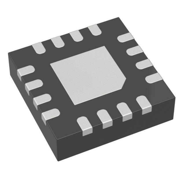
The LMK1D2102RGTT is a high-performance clock buffer designed by Texas Instruments, ideal for applications requiring precise timing and high-frequency performance. This device is part of the Clock/Timing ICs category and features a 1:2 input-to-output ratio, providing two differential clock outputs from a single input. The LMK1D2102RGTT supports a wide range of input signal types, including CML, HCSL, LVCMOS, LVDS, and LVPECL, making it versatile for various electronic systems. It operates over multiple supply voltage ranges: 1.71V to 1.89V, 2.375V to 2.625V, and 3.135V to 3.465V, ensuring compatibility with different power supply configurations. The device is housed in a 16-pin VQFN package, suitable for surface-mount applications, and is available in a tape and reel (TR) packaging format. With a maximum operating frequency of 2 GHz, the LMK1D2102RGTT is well-suited for high-speed clock distribution and synchronization tasks. It is currently an active product, with an ECCN classification of EAR99 and an HTSUS code of 8542.39.0001. The moisture sensitivity level (MSL) is rated at 1 (Unlimited), indicating it is suitable for a wide range of environmental conditions.
LMK1D2102RGTT Features
- High-Frequency Performance: Capable of operating up to 2 GHz, the LMK1D2102RGTT ensures precise clock distribution and synchronization in high-speed systems.
- Versatile Input and Output Options: Supports multiple input signal types (CML, HCSL, LVCMOS, LVDS, LVPECL) and provides differential LVDS outputs, enhancing its compatibility with various electronic systems.
- Wide Supply Voltage Range: Operates over multiple voltage ranges (1.71V to 1.89V, 2.375V to 2.625V, and 3.135V to 3.465V), offering flexibility in power supply design.
- Surface-Mount Compatibility: The 16-pin VQFN package is ideal for surface-mount applications, facilitating integration into compact and high-density PCB designs.
- Robust Environmental Rating: With an MSL rating of 1 (Unlimited), the LMK1D2102RGTT is suitable for a wide range of environmental conditions, ensuring reliability in diverse applications.
- Active Product Status: As an active product, the LMK1D2102RGTT benefits from ongoing support and availability, providing long-term reliability for system designers.
LMK1D2102RGTT Applications
The LMK1D2102RGTT is ideal for a variety of high-speed clock distribution and synchronization applications. Its high-frequency performance and versatile input/output options make it suitable for:
- Communication Systems: Ensuring precise timing in high-speed data transmission systems.
- High-Performance Computing: Providing reliable clock distribution in multi-processor systems and high-speed memory interfaces.
- Networking Equipment: Facilitating accurate clock synchronization in routers, switches, and other networking devices.
- Consumer Electronics: Enhancing the performance of high-definition video processing and display systems.
- Industrial Automation: Ensuring reliable clock distribution in control systems and real-time processing applications.
Conclusion of LMK1D2102RGTT
The LMK1D2102RGTT from Texas Instruments is a robust and versatile clock buffer, offering high-frequency performance and wide compatibility with various input and output signal types. Its surface-mount package and wide supply voltage range make it suitable for a broad range of applications, from high-speed communication systems to industrial automation. With an active product status and a robust environmental rating, the LMK1D2102RGTT provides long-term reliability and performance, making it an excellent choice for designers seeking a high-performance clock buffer solution.
FAQ
| Quantity | Unit Price | Ext. Price |
|---|---|---|
| 1+ | $9.58320 | $9.58 |
| 10+ | $7.49672 | $74.97 |
| 25+ | $6.97558 | $174.39 |
| 100+ | $6.40279 | $640.28 |
| 250+ | $6.12980 | $1532.45 |
Not available to buy online? Want the lower wholesale price? Please Send RFQ to get best price, we will respond immediately


.png?x-oss-process=image/format,webp/resize,h_32)


