Texas Instruments_LMV324AQPWRQ1

Texas Instruments
LMV324AQPWRQ1  
OP Amps, Buffer Amps ICs

Texas Instruments
LMV324AQPWRQ1
687-LMV324AQPWRQ1
Ersa
Texas Instruments-LMV324AQPWRQ1-datasheets-1793141.pdf
IC OPAMP GP 4 CIRCUIT 14TSSOP
In Stock : 13247

Not available to buy online? Want the lower wholesale price? Please Send RFQ to get best price, we will respond immediately

QUICK RFQ
ADD TO RFQ LIST
ersa FreeSample ersa flow
  • Quantity
  • Unit Price
  • Ext. Price
    • 1+
    • $1.65103
    • $1.65
    • 10+
    • $1.46887
    • $14.69
    • 30+
    • $1.33970
    • $40.19
    ADD TO CART
    QUICK ORDER
    $1.65103    $1.65
    ISO9001
    Quality Policy
    ISO45001
    ISO14001

    LMV324AQPWRQ1 Description

    The LMV324AQPWRQ1 is a low-power, quad operational amplifier (op-amp) manufactured by Texas Instruments. It is designed for use in a wide range of applications, including precision data acquisition systems, battery-powered equipment, and portable devices.

    Description:

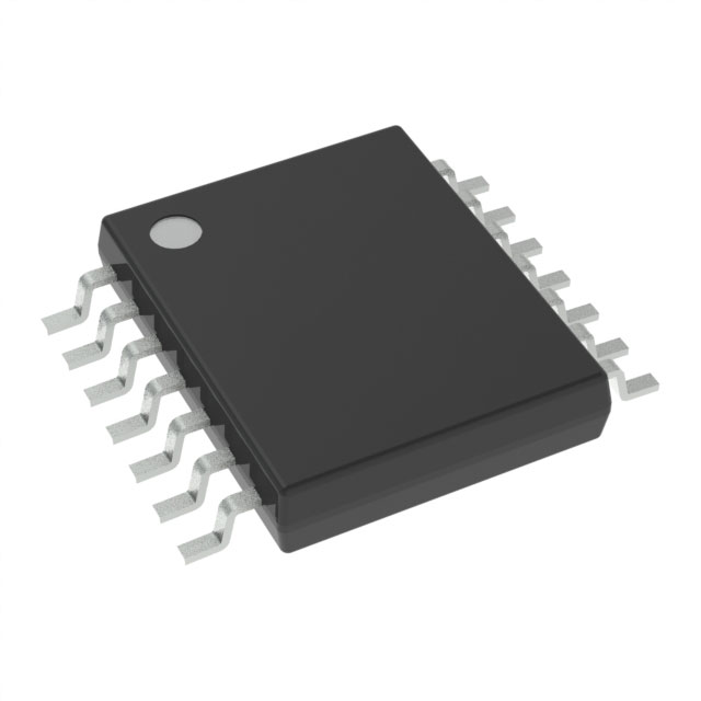
    The LMV324AQPWRQ1 is a 14-pin, quad, low-power operational amplifier package. It is available in a small-outline wide (SOIC) package, making it suitable for use in compact and portable devices.

    Features:

    1. Low power consumption: The LMV324AQPWRQ1 operates on a supply voltage range of 2.7V to 10V and has a low supply current of 330µA per amplifier, making it ideal for battery-powered applications.
    2. Precision performance: The device offers precision characteristics, including a low input offset voltage of 1mV max, low input bias current of 50pA max, and a high open-loop gain of 130dB min.
    3. Wide operating temperature range: The LMV324AQPWRQ1 can operate over a temperature range of -40°C to +125°C, making it suitable for use in harsh environments.
    4. Low noise: The op-amp features a low input voltage noise of 8.5nV/√Hz, which is beneficial for applications requiring low-noise performance.
    5. Rail-to-rail input and output: The LMV324AQPWRQ1 provides rail-to-rail input and output characteristics, allowing it to operate with input signals that are close to the supply voltage rails.

    Applications:

    1. Data acquisition systems: The LMV324AQPWRQ1's precision performance and low power consumption make it suitable for use in battery-powered data acquisition systems.
    2. Portable devices: The low power consumption and small package size of the LMV324AQPWRQ1 make it an ideal choice for portable devices, such as smartphones, wearables, and handheld instruments.
    3. Medical equipment: The low noise and precision characteristics of the LMV324AQPWRQ1 make it suitable for use in medical equipment, such as patient monitors and diagnostic devices.
    4. Industrial control systems: The LMV324AQPWRQ1 can be used in industrial control systems for signal conditioning and amplification of sensor signals.
    5. Audio equipment: The low noise and precision performance of the LMV324AQPWRQ1 make it suitable for use in audio equipment, such as preamplifiers and active filters.

    In summary, the LMV324AQPWRQ1 is a low-power, quad operational amplifier from Texas Instruments that offers precision performance, low power consumption, and a wide operating temperature range. It is suitable for use in a variety of applications, including data acquisition systems, portable devices, medical equipment, industrial control systems, and audio equipment.

    Tech Specifications

    Number of Channels per Chip
    Rail-to-rail
    Product
    PPAP
    Gain Bandwidth Product
    Automotive
    RoHS
    THD plus Noise
    REACH Status
    Input common mode headroom (to negative supply) (typ) (V)
    Operating temperature range (°C)
    PSRR - Power Supply Rejection Ratio
    Supplier Temperature Grade
    Current - Supply
    Output swing headroom (to negative supply) (typ) (V)
    Standard Package Name
    Shut Down Support
    Mounting
    Qualification
    Minimum Single Supply Voltage (V)
    Iout (typ) (A)
    Manufacturer Type
    Package
    Minimum CMRR (dB)
    Maximum Quiescent Current (mA)
    Total supply voltage (+5 V = 5, ±5 V = 10) (max) (V)
    GBW (typ) (MHz)
    en - Input Voltage Noise Density
    Output Type
    Vos - Input Offset Voltage
    Minimum CMRR Range (dB)
    Typical Gain Bandwidth Product (MHz)
    Package Height
    Maximum Operating Temperature
    Ib - Input Bias Current
    RoHS Status
    Number of channels
    Iq per channel (typ) (mA)
    Minimum Operating Temperature
    Voltage - Input Offset
    Type
    Vos (offset voltage at 25°C) (max) (mV)
    Part Status
    Lead finish / Ball material
    Number of Circuits
    Package Width
    GBP - Gain Bandwidth Product
    Maximum Input Offset Voltage (mV)
    Product Status
    Current - Input Bias
    Rail to Rail
    Supplier Package
    Package / Case
    Number of Channels
    Typical Voltage Gain (dB)
    Typical Input Bias Current (uA)
    EU RoHS
    Carrier
    Amplifier Type
    Maximum Dual Supply Voltage (V)
    Input common mode headroom (to positive supply) (typ) (V)
    Moisture Sensitivity Level (MSL)
    Typical Input Noise Voltage Density (nV/rtHz)
    Operating Temperature
    Architecture
    Typical Slew Rate (V/us)
    Output swing headroom (to positive supply) (typ) (V)
    ECCN
    Grade
    MSL rating / Peak reflow
    Mounting Type
    Pin Count
    In - Input Noise Current Density
    Ios - Input Offset Current
    Minimum PSRR (dB)
    Shutdown
    HTSUS
    Pins
    Current - Output / Channel
    USHTS
    PCB changed
    HTS
    Rating
    ECCN (US)
    Total supply voltage (+5 V = 5, ±5 V = 10) (min) (V)
    Supplier Device Package
    Supply Voltage - Min
    Minimum Operating Temperature (°C)
    Maximum Operating Temperature (°C)
    SR - Slew Rate
    Mfr
    Features
    CMRR (typ) (dB)
    Supply Voltage - Max
    Offset drift (typ) (µV/°C)
    Mounting Style
    Input Type
    Typical Noninverting Input Current Noise Density (pA/rtHz)
    Slew Rate
    Package Length
    Minimum Dual Supply Voltage (V)
    Vn at 1 kHz (typ) (nV√Hz)
    CMRR - Common Mode Rejection Ratio
    REACH
    Series
    Maximum Single Supply Voltage (V)
    Slew rate (typ) (V/µs)
    Typical Settling Time (ns)

    LMV324AQPWRQ1 Documents

    Download datasheets and manufacturer documentation for LMV324AQPWRQ1

    Ersa LMV324A-Q1, LMV358A-Q1      
    Ersa Symbolization Update 28/Nov/2022      
    Ersa LMV324A-Q1, LMV358A-Q1      
    Ersa Design 22/Feb/2022      

    Shopping Guide

    Payment Methods
    Payment Methods include Prepayment TT (bank transfer), Western Union, and PayPal. Customers are responsible for shipping costs, bank charges, customs duties and taxes.
    Shipping Rate
    Shipments are made once a day around 5pm, excluding Sundays. Once shipped, the estimated delivery time is usually 5-7 business days, depending on the courier you choose.
    Delivery Methods
    Provide DHL, FedEx, UPS, EMS, SF Express and Registered Airmail International Delivery Service