
Texas Instruments
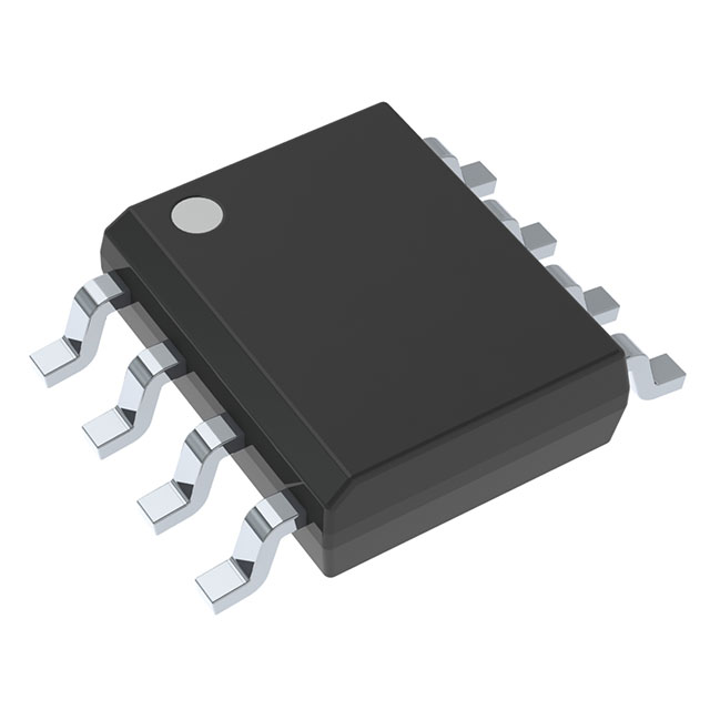
LMV358ID
OP Amps, Buffer Amps ICs


.png?x-oss-process=image/format,webp/resize,p_30)


LMV358ID Description
LMV358ID Description
The LMV358ID is a dual operational amplifier (op-amp) from Texas Instruments, designed for general-purpose applications. It features a wide supply voltage range of 2.7 V to 5.5 V, making it suitable for a variety of low-voltage systems. With a gain bandwidth product of 1 MHz, it offers high-speed performance for demanding applications. The LMV358ID is compliant with RoHS3 and REACH regulations, ensuring environmentally friendly manufacturing.
LMV358ID Features
- Wide Supply Voltage Range: 2.7 V to 5.5 V, ideal for low-voltage systems.
- High Gain Bandwidth Product: 1 MHz, suitable for high-speed applications.
- Low Input Bias Current: 15 nA, minimizing input offset errors.
- Low Input Offset Voltage: 1.7 mV, improving accuracy in precision applications.
- High Slew Rate: 1 V/µs, enabling fast response times.
- Low Supply Current: 210 µA (x2 channels), reducing power consumption in battery-powered devices.
- High Output Current: 40 mA per channel, capable of driving demanding loads.
- Surface Mount Packaging:。
- Dual Channel Operation:, op-amp 。
LMV358ID Applications
The LMV358ID is ideal for a variety of applications where low-voltage operation, high-speed performance, and precision are required. Some specific use cases include:
- Audio Amplification: Utilizing its low distortion and high slew rate, the LMV358ID is perfect for audio signal amplification in consumer electronics.
- Sensor Signal Conditioning: Its low input bias current and low input offset voltage make it suitable for conditioning signals from sensors in industrial and automotive applications.
- Battery-Powered Devices: The low supply current of the LMV358ID extends battery life in portable electronics and IoT devices.
- Data Acquisition Systems: The LMV358ID's high gain bandwidth product and low noise characteristics make it suitable for amplifying and filtering signals in data acquisition systems.
Conclusion of LMV358ID
The LMV358ID from Texas Instruments is a versatile, dual-channel operational amplifier designed for low-voltage, high-speed applications. Its combination of wide supply voltage range, high gain bandwidth product, and low power consumption make it an ideal choice for a variety of applications, including audio amplification, sensor signal conditioning, and battery-powered devices. With its RoHS3 and REACH compliance, the LMV358ID is also an environmentally friendly option for designers looking to meet regulatory requirements.
Tech Specifications
LMV358ID Documents
Download datasheets and manufacturer documentation for LMV358ID
 Material Set Revision A 12/Mar/2014
  LMV321, 324, 358 Datasheet
  LM324/LM358 obs 23/Feb/2023
  Design 25/Feb/2022 Mult Dev 27/Jul/2023
 Shopping Guide


.png?x-oss-process=image/format,webp/resize,h_32)


