
Texas Instruments
LMV358IDRQ1
OP Amps, Buffer Amps ICs


.png?x-oss-process=image/format,webp/resize,p_30)


LMV358IDRQ1 Description
LMV358IDRQ1 Description
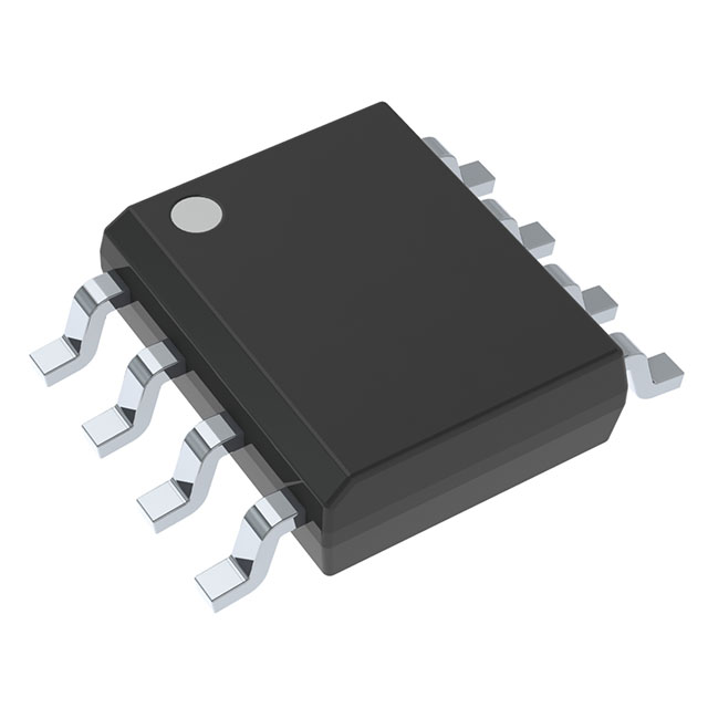
The LMV358IDRQ1 is a general-purpose operational amplifier (op-amp) from Texas Instruments, designed for a wide range of applications requiring high performance and reliability. This dual-channel op-amp is housed in an 8-pin SOIC package, making it suitable for surface-mount technology (SMT) applications. The LMV358IDRQ1 operates with a supply voltage range of 2.7 V to 5.5 V, making it ideal for low-voltage systems. It features a gain bandwidth product of 1 MHz and a slew rate of 1 V/µs, ensuring stable and precise signal processing.
LMV358IDRQ1 Features
- Supply Voltage Range: The LMV358IDRQ1 operates within a wide supply voltage range of 2.7 V to 5.5 V, making it suitable for both low-voltage and standard voltage applications.
- Gain Bandwidth Product: With a gain bandwidth product of 1 MHz, this op-amp provides excellent performance for applications requiring high-frequency signal processing.
- Low Input Bias Current: The low input bias current of 15 nA ensures minimal loading on the input signal source, maintaining signal integrity.
- High Slew Rate: A slew rate of 1 V/µs allows for fast response times, making it suitable for applications requiring rapid signal transitions.
- Low Supply Current: The low supply current of 210 µA per channel (x2 channels) ensures efficient power usage, making it ideal for battery-powered and low-power applications.
- Low Input Offset Voltage: The input offset voltage of 1.7 mV ensures high accuracy and precision in signal amplification.
- High Output Current: Each channel can deliver up to 160 mA of output current, providing robust performance for driving various loads.
- Compliance and Packaging: The LMV358IDRQ1 is REACH unaffected and RoHS3 compliant, ensuring environmental safety. It is available in a tape & reel (TR) package, facilitating easy handling and assembly in automated manufacturing processes.
LMV358IDRQ1 Applications
The LMV358IDRQ1 is versatile and can be used in a variety of applications, including:
- Signal Conditioning: Ideal for amplifying and conditioning low-level signals in sensor interfaces, ensuring accurate and reliable signal transmission.
- Analog Filters: Its high gain bandwidth product and low input offset voltage make it suitable for designing active filters with precise frequency response characteristics.
- Transimpedance Amplifiers: The low input bias current and high slew rate make it perfect for converting current signals to voltage in photodiode and other current-output sensors.
- General-Purpose Amplification: Suitable for a wide range of general-purpose amplification tasks, including audio and instrumentation applications.
- Power Management: The low supply current and high output current capability make it ideal for use in power management circuits, such as voltage regulators and motor drivers.
Conclusion of LMV358IDRQ1
The LMV358IDRQ1 from Texas Instruments is a robust and versatile general-purpose op-amp that offers high performance and reliability in a compact 8-pin SOIC package. Its wide supply voltage range, low input bias current, high slew rate, and low supply current make it an excellent choice for a variety of applications, from signal conditioning to power management. Despite being marked as obsolete, the LMV358IDRQ1 remains a reliable option for engineers and designers seeking a high-performance op-amp for their projects.
Tech Specifications
LMV358IDRQ1 Documents
Download datasheets and manufacturer documentation for LMV358IDRQ1
Shopping Guide


.png?x-oss-process=image/format,webp/resize,h_32)


