
Texas Instruments
LMV358M/NOPB
OP Amps, Buffer Amps ICs


.png?x-oss-process=image/format,webp/resize,p_30)


LMV358M/NOPB Description
LMV358M/NOPB Description
The LMV358M/NOPB is a dual general-purpose operational amplifier from Texas Instruments, designed for a wide range of applications requiring high performance and reliability. This IC is part of the LMV® series, known for its robustness and versatility. The LMV358M/NOPB operates from a supply voltage range of 2.7 V to 5.5 V, making it suitable for both low-voltage and standard voltage applications. It features a gain bandwidth product of 1 MHz, ensuring stable performance across a broad frequency spectrum. The amplifier's slew rate of 1 V/µs allows for rapid response times, crucial for dynamic signal processing.
LMV358M/NOPB Features
- Wide Supply Voltage Range: Operates from 2.7 V to 5.5 V, providing flexibility in power supply design.
- Low Input Bias Current: 15 nA ensures minimal loading on the input signal source, preserving signal integrity.
- High Output Current: Each channel can deliver up to 160 mA, making it suitable for driving heavy loads.
- Low Input Offset Voltage: 1.7 mV ensures high accuracy in signal amplification and processing.
- Dual Channel Design: Two independent operational amplifiers in a single package, optimizing space and cost.
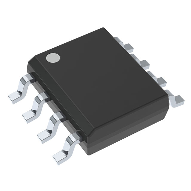
- Surface Mount Packaging: The 8SOIC package is ideal for compact and high-density PCB designs.
- Compliance and Reliability: REACH unaffected and ROHS3 compliant, ensuring environmental and regulatory standards are met.
- Moisture Sensitivity Level: MSL 1 (Unlimited) indicates excellent resistance to moisture, enhancing reliability in various environmental conditions.
LMV358M/NOPB Applications
The LMV358M/NOPB is well-suited for a variety of applications, including:
- Signal Conditioning: Ideal for amplifying and conditioning weak signals in sensor interfaces and transducers.
- Filter Design: Suitable for active filter applications, providing precise signal filtering and processing.
- Power Management: Effective in voltage regulation and power supply circuits, ensuring stable power delivery.
- Consumer Electronics: Used in audio amplifiers, video signal processing, and other consumer devices requiring high performance and reliability.
- Industrial Automation: Reliable for control systems, signal processing, and instrumentation where precision and robustness are critical.
Conclusion of LMV358M/NOPB
The LMV358M/NOPB from Texas Instruments is a versatile and high-performance dual operational amplifier that stands out in its class. Its wide supply voltage range, low input bias current, and high output current make it suitable for a broad range of applications. The dual-channel design in a compact 8SOIC package optimizes space and cost, while compliance with environmental and regulatory standards ensures long-term reliability. Whether used in signal conditioning, power management, or consumer electronics, the LMV358M/NOPB offers superior performance and reliability, making it an excellent choice for engineers and designers in the electronics industry.
Tech Specifications
LMV358M/NOPB Documents
Download datasheets and manufacturer documentation for LMV358M/NOPB
 Metal One Composition Update 17/Jul/2014
  LMV321,358,324,(-N,N-Q1)
  LMV321,358,324,(-N,N-Q1)
  LMV3yy 15/Sep/2020 SOIC Pkg Wire Bonding 20/Mar/2013
 Shopping Guide


.png?x-oss-process=image/format,webp/resize,h_32)


