
Texas Instruments
LMV358Q1MM/NOPB
OP Amps, Buffer Amps ICs


.png?x-oss-process=image/format,webp/resize,p_30)


LMV358Q1MM/NOPB Description
The LMV358Q1MM/NOPB is a low-power, low-noise operational amplifier (op-amp) from Texas Instruments. It is designed to provide high performance in a small package, making it ideal for a wide range of applications.
Description:
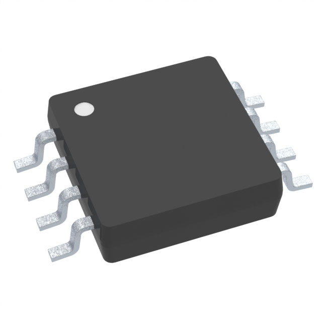
The LMV358Q1MM/NOPB is an 8-pin SOIC (Small Outline Integrated Circuit) package that features a single op-amp. It is designed to operate over a wide supply voltage range of 2.7V to 10V and has a quiescent current of only 50µA. The device is specified for operation over a temperature range of -40°C to +125°C.
Features:
- Low Input Bias Current: The LMV358Q1MM/NOPB has an input bias current of only 2pA, which makes it suitable for high-impedance input applications.
- Low Input Offset Voltage: The input offset voltage is typically 1mV, which is very low and helps to improve the accuracy of the device.
- Low Noise: The device has a low input voltage noise of 7nV/√Hz, which is beneficial for precision applications.
- High Slew Rate: The LMV358Q1MM/NOPB has a high slew rate of 0.8V/µs, which allows it to respond quickly to input changes.
- Wide Supply Voltage Range: The device can operate over a wide supply voltage range of 2.7V to 10V, making it suitable for a variety of power supply configurations.
- Small Package: The 8-pin SOIC package is compact and easy to integrate into a variety of applications.
Applications:
The LMV358Q1MM/NOPB is suitable for a wide range of applications, including:
- Audio Amplification: The low noise and high slew rate make it ideal for audio amplification applications.
- Strain Gauge Amplification: The low input bias current and low noise make it suitable for use with strain gauges in measurement and control systems.
- Battery Monitors: The low quiescent current makes it ideal for battery monitoring applications where power consumption is critical.
- Medical Instruments: The low noise and low input bias current make it suitable for use in medical instruments where precision is important.
- Industrial Control Systems: The LMV358Q1MM/NOPB can be used in a variety of industrial control systems, including motor control and sensor conditioning.
Overall, the LMV358Q1MM/NOPB is a high-performance, low-power op-amp that is suitable for a wide range of applications where precision and low noise are important. Its small package and wide supply voltage range make it easy to integrate into a variety of systems.
Tech Specifications
LMV358Q1MM/NOPB Documents
Download datasheets and manufacturer documentation for LMV358Q1MM/NOPB
 Wafer Metal Update 2/Dec/2016
  LMV321,324,358(-Q1) Datasheet
  LMV321,324,358(-Q1) Datasheet
  LMV3yy 15/Sep/2020
 Shopping Guide


.png?x-oss-process=image/format,webp/resize,h_32)


