
 German
 Japanese
 Portuguese
 Korea
Korea
 Mexico
 Dutch
Dutch


Texas Instruments
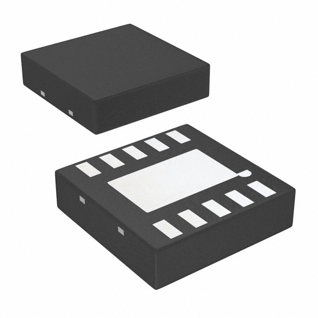
LMV712LD

Why Choose Us?
Professional Platform
B2B & B2C purchasingDelivery at full speed
1-2 days deliveryWide variety
Original manufacturers365 days guarantee
Responsible quality
.png)


Tech Specifications
LMV712LD Description
LMV712LD Description
The LMV712LD is a general-purpose operational amplifier (op-amp) from Texas Instruments, designed for applications requiring high performance in a compact package. This dual-channel op-amp is part of the LMV® series, known for its versatility and reliability. The LMV712LD operates within a wide supply voltage range of 2.7 V to 5.5 V, making it suitable for a variety of power supply configurations. It features a gain bandwidth product of 5 MHz, providing excellent frequency response for signal processing tasks. The device also boasts a high slew rate of 5V/µs, ensuring fast transient response and minimal distortion in high-frequency applications.
LMV712LD Features
- Wide Supply Voltage Range: The LMV712LD operates from 2.7 V to 5.5 V, offering flexibility in power supply design.
- High Gain Bandwidth Product: With a 5 MHz gain bandwidth product, this op-amp is ideal for applications requiring high-frequency signal processing.
- Low Input Bias Current: The low input bias current of 5.5 pA ensures minimal loading on input sources, preserving signal integrity.
- High Slew Rate: The 5V/µs slew rate allows for fast transient response, making it suitable for high-speed applications.
- Low Input Offset Voltage: The 400 µV input offset voltage ensures accurate signal amplification with minimal error.
- Dual-Channel Design: The LMV712LD features two independent op-amp channels, each capable of sourcing up to 50 mA of output current, providing flexibility in multi-channel applications.
- Surface Mount Packaging: The device is available in a surface mount package, making it suitable for automated assembly processes and compact designs.
- Moisture Sensitivity Level 1: The MSL 1 rating indicates that the device is moisture insensitive, ensuring reliability in various environmental conditions.
- Compliance: The LMV712LD is REACH unaffected and classified under ECCN EAR99, ensuring compliance with international regulations.
LMV712LD Applications
The LMV712LD is well-suited for a variety of applications due to its high performance and versatility. Some specific use cases include:
- Signal Conditioning: The wide supply voltage range and high slew rate make it ideal for conditioning signals in industrial control systems and instrumentation.
- Audio Applications: The low input offset voltage and high gain bandwidth product ensure high-fidelity audio signal processing.
- Power Management: The dual-channel design allows for efficient power management in multi-channel systems, such as battery management circuits.
- Consumer Electronics: The compact surface mount package and high performance make it suitable for consumer electronics where space is limited.
- Automotive Electronics: The moisture sensitivity level 1 rating ensures reliability in automotive environments, making it suitable for automotive control units and sensor interfaces.
Conclusion of LMV712LD
The LMV712LD from Texas Instruments is a robust and versatile general-purpose op-amp that offers high performance in a compact package. Its wide supply voltage range, high gain bandwidth product, and low input bias current make it suitable for a variety of applications, from signal conditioning to audio processing. The dual-channel design and high slew rate provide additional flexibility, making it an excellent choice for multi-channel systems. Despite being marked as obsolete, the LMV712LD remains a reliable option for engineers seeking a high-performance op-amp with proven reliability and compliance.
FAQ
Not available to buy online? Want the lower wholesale price? Please Send RFQ to get best price, we will respond immediately


.png?x-oss-process=image/format,webp/resize,h_32)


