
Texas Instruments
LMV822DR
OP Amps, Buffer Amps ICs


.png?x-oss-process=image/format,webp/resize,p_30)


LMV822DR Description
LMV822DR Description
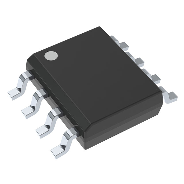
The LMV822DR is an operational amplifier (op-amp) designed and manufactured by Texas Instruments. It is part of the LMV® series and is classified as a general-purpose amplifier. The LMV822DR is an obsolete product, but it still offers a range of features that make it suitable for various applications. It is a dual-channel op-amp, meaning it has two independent op-amp circuits in a single package. The device is surface-mountable and is packaged in an 8-SOIC package.
LMV822DR Features
- Voltage Supply Span: The LMV822DR operates over a wide voltage range, from a minimum of 2.5 V to a maximum of 5.5 V. This makes it suitable for a variety of power supply configurations.
- Gain Bandwidth Product: The LMV822DR has a gain bandwidth product of 5.5 MHz, allowing it to amplify signals with frequencies up to 5.5 MHz.
- Slew Rate: The device has a slew rate of 1.9 V/µs, which is the maximum rate at which the output voltage can change in response to an input signal.
- Input Bias Current: The LMV822DR has an input bias current of 40 nA, which is relatively low, making it suitable for applications where low input current is required.
- Voltage Input Offset: The LMV822DR has a voltage input offset of 1 mV, which is the difference between the two input voltages required to produce a zero output voltage.
- Supply Current: The LMV822DR consumes a supply current of 500 µA, which is relatively low, making it suitable for power-sensitive applications.
- Output Current per Channel: Each channel of the LMV822DR can provide an output current of 45 mA.
- RoHS Compliance: The LMV822DR is compliant with the RoHS3 directive, which restricts the use of hazardous substances in electronic products.
- REACH Status: The LMV822DR is unaffected by the Registration, Evaluation, Authorization, and Restriction of Chemicals (REACH) regulation.
- Moisture Sensitivity Level: The LMV822DR has a moisture sensitivity level of 1 (unlimited), which means it can be stored and handled without special precautions for moisture sensitivity.
LMV822DR Applications
The LMV822DR is a versatile op-amp that can be used in a variety of applications, including:
- Audio and video processing: The LMV822DR's wide bandwidth and low distortion make it suitable for audio and video signal processing applications.
- Sensor conditioning: The LMV822DR's low input bias current and low voltage offset make it suitable for conditioning signals from sensors, such as temperature, pressure, and humidity sensors.
- Instrumentation: The LMV822DR can be used in instrumentation applications, such as signal amplification and filtering in data acquisition systems.
- Industrial control: The LMV822DR can be used in industrial control applications, such as motor control and process control systems.
Conclusion of LMV822DR
The LMV822DR is a dual-channel, general-purpose op-amp from Texas Instruments that offers a range of features, including a wide voltage supply range, high gain bandwidth product, and low input bias current. Although it is now considered obsolete, it still offers performance benefits that make it suitable for a variety of applications, including audio and video processing, sensor conditioning, instrumentation, and industrial control. Its RoHS compliance and REACH unaffected status also make it suitable for use in environmentally conscious applications.
Tech Specifications
LMV822DR Documents
Download datasheets and manufacturer documentation for LMV822DR
 LMV821,22,24
  Multiple Devices 18/May/2012
  LMV821,22,24
 Shopping Guide


.png?x-oss-process=image/format,webp/resize,h_32)


