
Texas Instruments
LMV931QDBVRQ1
OP Amps, Buffer Amps ICs


.png?x-oss-process=image/format,webp/resize,p_30)


LMV931QDBVRQ1 Description
LMV931QDBVRQ1 Description
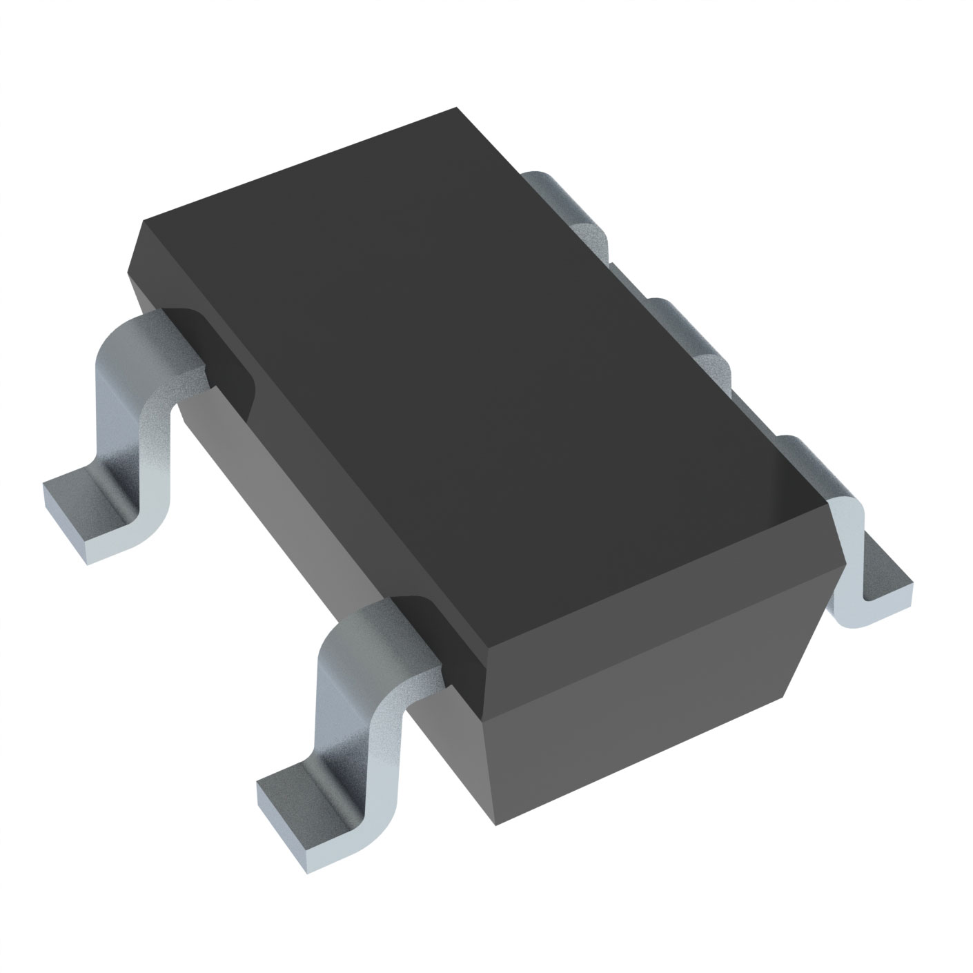
The LMV931QDBVRQ1 is a general-purpose operational amplifier designed for automotive applications, manufactured by Texas Instruments. This IC features a wide supply voltage range from 1.8 V to 5 V, making it suitable for various power supply environments. It offers a gain bandwidth product of 1.5 MHz and a slew rate of 0.42 V/µs, ensuring high performance in signal processing applications. The LMV931QDBVRQ1 is housed in a compact SOT23-5 package, ideal for surface mount applications where space is a constraint.
LMV931QDBVRQ1 Features
- Wide Supply Voltage Range: Operates from 1.8 V to 5 V, providing flexibility in various power supply configurations.
- Low Input Bias Current: With an input bias current of only 15 nA, this op-amp minimizes offset errors in high-impedance circuits.
- Low Supply Current: Consumes only 116 µA of supply current, making it energy-efficient for low-power applications.
- High Output Current: Capable of delivering up to 100 mA per channel, suitable for driving heavy loads.
- Low Input Offset Voltage: Features an input offset voltage of 1 mV, ensuring accurate signal amplification.
- Automotive Grade: Certified for automotive applications, ensuring reliability and performance in demanding environments.
- Compliance: REACH unaffected and RoHS3 compliant, meeting environmental and regulatory standards.
- Moisture Sensitivity Level: MSL 1 (Unlimited), suitable for storage and handling in various conditions.
LMV931QDBVRQ1 Applications
The LMV931QDBVRQ1 is ideal for a variety of applications, particularly in the automotive sector, where reliability and performance are critical. Its wide supply voltage range and low power consumption make it suitable for battery-powered systems. The high output current capability allows it to drive actuators and sensors directly. Its low input bias current and offset voltage make it ideal for precision signal conditioning in sensor interfaces and analog signal processing circuits.
Conclusion of LMV931QDBVRQ1
The LMV931QDBVRQ1 is a versatile and reliable operational amplifier designed for automotive applications. Its wide supply voltage range, low power consumption, and high output current make it suitable for a variety of demanding environments. While it is currently marked as obsolete, its technical specifications and performance benefits continue to make it a valuable component for existing designs and legacy systems. For new projects, engineers may consider its successor models or similar alternatives that offer comparable or enhanced features.
Tech Specifications
LMV931QDBVRQ1 Documents
Download datasheets and manufacturer documentation for LMV931QDBVRQ1
Shopping Guide


.png?x-oss-process=image/format,webp/resize,h_32)


