
Texas Instruments
LP38693SD-ADJ/NOPB
Linear & Switching Voltage Regulators


- 1+
- $1.69574
- $1.7
- 10+
- $1.44900
- $14.49
- 30+
- $1.29499
- $38.85

.png?x-oss-process=image/format,webp/resize,p_30)


LP38693SD-ADJ/NOPB Description
The LP38693SD-ADJ/NOPB is a low-power, high-efficiency step-down (buck) switching regulator from Texas Instruments. It is designed to provide a stable and regulated output voltage from a wide range of input voltages. Here is a brief description of the device, its features, and potential applications:
Description:
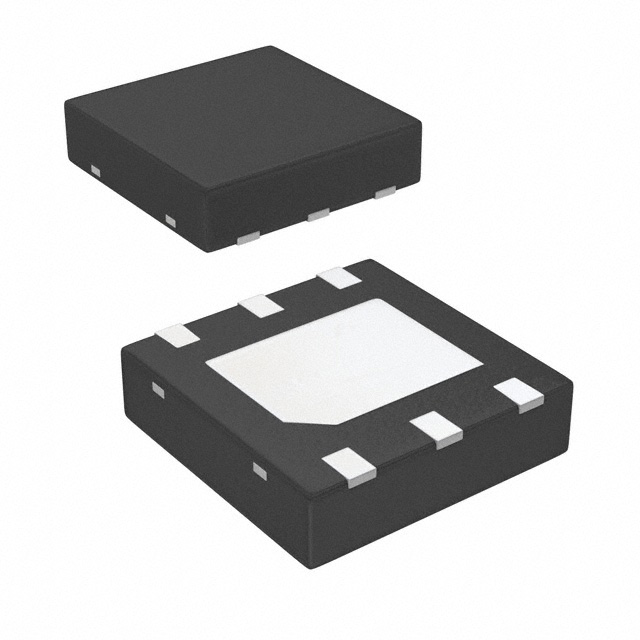
The LP38693SD-ADJ/NOPB is a compact, high-performance step-down converter that can efficiently step down a higher input voltage to a lower, regulated output voltage. It is available in a small, thermally-optimized DFN package, making it suitable for space-constrained applications.
Features:
- Adjustable Output Voltage: The output voltage can be adjusted using an external resistor divider, allowing for customization to meet specific voltage requirements.
- Wide Input Voltage Range: The device can handle input voltages from 2.5V to 5.5V, making it versatile for a range of power supply scenarios.
- High Efficiency: It offers high efficiency of up to 95%, which is crucial for battery-powered devices to extend battery life.
- Low Quiescent Current: The device has a low quiescent current (Iq) of 2.5μA in normal operation and 1μA in ultra-low power shutdown mode, which is beneficial for power-sensitive applications.
- Small Package Size: The DFN (Dual Flat No-leads) package is compact, making it suitable for portable and space-constrained designs.
- Protection Features: It includes over-current protection (OCP), over-voltage protection (OVP), and thermal shutdown protection to safeguard against fault conditions.
- Soft Start: The soft-start feature minimizes inrush current and reduces output voltage overshoot during startup.
Applications:
- Portable Devices: Due to its low power consumption and efficiency, it is ideal for use in portable electronics like smartphones, tablets, and wearable devices.
- IoT Devices: The LP38693SD-ADJ/NOPB is suitable for powering Internet of Things (IoT) devices where energy efficiency and compact size are critical.
- Medical Devices: Its low noise and high efficiency make it a good choice for battery-powered medical equipment.
- Industrial Equipment: The device can be used in industrial applications where a regulated power supply is required, such as in sensors and control systems.
- Consumer Electronics: It can also be used in various consumer electronics, including cameras, GPS devices, and portable gaming systems.
When using the LP38693SD-ADJ/NOPB, it's important to carefully consider the specific requirements of the application, such as the desired output voltage, input voltage range, and power efficiency, to ensure the device meets the design needs.
Tech Specifications
LP38693SD-ADJ/NOPB Documents
Download datasheets and manufacturer documentation for LP38693SD-ADJ/NOPB
 Qualification Assembly/Test Site 27/Dec/2013
  LP38691/93-ADJ
  LP38691/93-ADJ
  Data Sheet Chg 3/Feb/2016 Wire Base Metal 05/Oct/2016
 Shopping Guide


.png?x-oss-process=image/format,webp/resize,h_32)


