
 German
 Japanese
 Portuguese
 Korea
Korea
 Mexico
 Dutch
Dutch


Texas Instruments
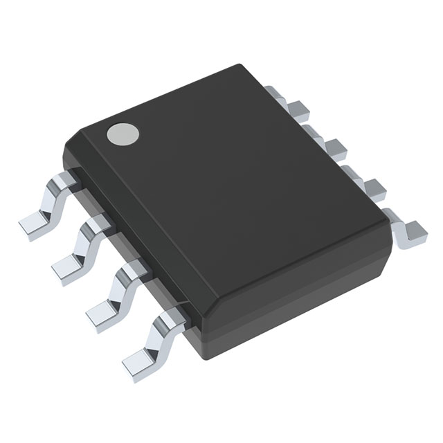
LPC662AIM

Why Choose Us?
Professional Platform
B2B & B2C purchasingDelivery at full speed
1-2 days deliveryWide variety
Original manufacturers365 days guarantee
Responsible quality
.png)


Tech Specifications
LPC662AIM Description
LPC662AIM Description
The LPC662AIM is a high-performance CMOS operational amplifier designed by Texas Instruments, featuring a dual-channel configuration in a surface-mount package. This IC is optimized for low power consumption and high precision, making it suitable for a wide range of applications in the electronics industry. With a supply voltage range of 4.75 V to 15.5 V, the LPC662AIM offers flexibility in power supply options. Its gain bandwidth product of 350 kHz ensures stable performance across various frequencies. The amplifier boasts a low input bias current of 0.002 pA, which minimizes the loading effect on the input signal source, and a low input offset voltage of 1 mV, contributing to high accuracy in signal processing.
LPC662AIM Features
- Amplifier Type: CMOS
- Number of Circuits: 2
- Mounting Type: Surface Mount
- Package: Tube
- Voltage - Supply Span (Min/Max): 4.75 V / 15.5 V
- Gain Bandwidth Product: 350 kHz
- Slew Rate: 0.11 V/µs
- Current - Input Bias: 0.002 pA
- Voltage - Input Offset: 1 mV
- Current - Supply: 86µA (x2 Channels)
- Current - Output / Channel: 40 mA
- Moisture Sensitivity Level (MSL): 1 (Unlimited)
- REACH Status: REACH Unaffected
- RoHS Status: ROHS3 Compliant
- ECCN: EAR99
- HTSUS: 8542.33.0001
LPC662AIM Applications
The LPC662AIM is ideal for applications requiring low power consumption and high precision. Its low input bias current and low input offset voltage make it suitable for high-impedance signal sources and precision signal conditioning. The dual-channel configuration allows for efficient use in multi-signal processing applications. Some specific use cases include:
- Precision Signal Amplification: Ideal for amplifying weak signals in sensors and transducers.
- Analog-to-Digital Conversion: Enhances the performance of ADCs by providing a clean and amplified signal.
- Battery-Powered Devices: Suitable for applications where low power consumption is critical, such as portable electronics.
- Medical Equipment: Can be used in medical devices where high precision and low noise are essential.
Conclusion of LPC662AIM
The LPC662AIM from Texas Instruments is a versatile and high-performance CMOS operational amplifier designed for low power and high precision applications. Its dual-channel configuration, low input bias current, and low input offset voltage make it a superior choice for precision signal processing. The LPC662AIM is particularly well-suited for applications in precision signal amplification, analog-to-digital conversion, and battery-powered devices. With its compliance to REACH and RoHS3 standards, the LPC662AIM ensures environmental sustainability and regulatory adherence. For engineers and designers seeking a reliable and high-performance operational amplifier, the LPC662AIM is an excellent choice.
FAQ
Not available to buy online? Want the lower wholesale price? Please Send RFQ to get best price, we will respond immediately


.png?x-oss-process=image/format,webp/resize,h_32)


