
 German
 Japanese
 Portuguese
 Korea
Korea
 Mexico
 Dutch
Dutch


Texas Instruments
MAX4596DBVR

Why Choose Us?
Professional Platform
B2B & B2C purchasingDelivery at full speed
1-2 days deliveryWide variety
Original manufacturers365 days guarantee
Responsible quality
.png)


Tech Specifications
MAX4596DBVR Description
MAX4596DBVR Description
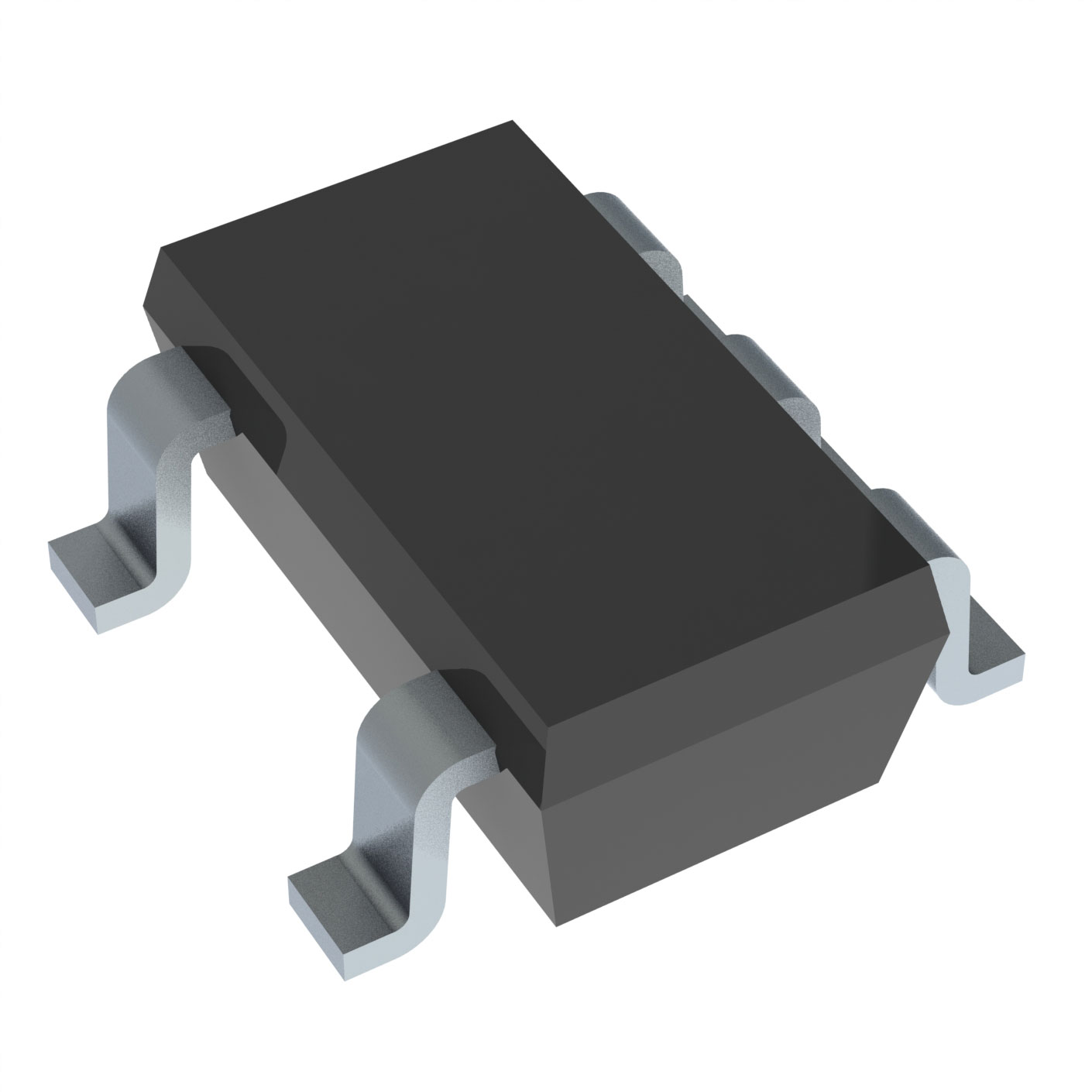
The MAX4596DBVR is a high-performance, single-pole single-throw (SPST) analog switch designed by Texas Instruments. This device is part of the MAX4596 family and is optimized for a wide range of applications requiring low on-state resistance, fast switching times, and minimal signal distortion. The MAX4596DBVR is housed in a compact SOT23 package, making it ideal for space-constrained designs.
MAX4596DBVR Features
- Low On-State Resistance: The MAX4596DBVR boasts a maximum on-state resistance of 10Ω, ensuring minimal power loss and high efficiency in signal transmission.
- Fast Switching Times: With a turn-on time of 35ns and a turn-off time of 40ns, the MAX4596DBVR provides rapid switching capabilities, making it suitable for high-speed applications.
- Wide Supply Voltage Range: The device operates over a wide supply voltage range of 2.4V to 5.5V, offering flexibility in power supply options.
- Low Leakage Current: The MAX4596DBVR has a maximum leakage current of 500pA, ensuring minimal signal degradation and power consumption.
- Low Channel Capacitance: With channel capacitance values of 8pF for both CS(off) and CD(off), the MAX4596DBVR minimizes signal distortion and ensures high-frequency performance.
- High Bandwidth: The -3dB bandwidth of 300MHz makes the MAX4596DBVR suitable for high-frequency analog signal routing.
- Minimal Charge Injection: The device exhibits a low charge injection of 2pC, which is crucial for maintaining signal integrity in sensitive analog circuits.
- Compliance and Packaging: The MAX4596DBVR is REACH unaffected and RoHS3 compliant, ensuring environmental sustainability. It is available in a surface-mount SOT23 package, which is ideal for automated assembly processes.
MAX4596DBVR Applications
The MAX4596DBVR is well-suited for a variety of applications where high performance and reliability are critical. Some specific use cases include:
- Analog Signal Routing: Ideal for routing analog signals in communication systems, test and measurement equipment, and medical devices.
- High-Speed Data Switching: Suitable for applications requiring fast data switching, such as in high-speed data acquisition systems and digital-to-analog converters.
- Audio Signal Processing: The low on-state resistance and minimal signal distortion make it suitable for audio signal routing in consumer electronics and professional audio equipment.
- Industrial Control Systems: The wide supply voltage range and robust performance make it suitable for industrial control systems where reliability and precision are paramount.
Conclusion of MAX4596DBVR
The MAX4596DBVR from Texas Instruments is a versatile and high-performance analog switch that offers significant advantages over similar models. Its low on-state resistance, fast switching times, and minimal signal distortion make it an ideal choice for a wide range of applications. The device's compliance with environmental standards and its compact surface-mount package further enhance its appeal for modern electronic designs. Whether used in high-speed data switching, analog signal routing, or audio processing, the MAX4596DBVR delivers reliable performance and exceptional value.
FAQ
Not available to buy online? Want the lower wholesale price? Please Send RFQ to get best price, we will respond immediately


.png?x-oss-process=image/format,webp/resize,h_32)


