
 German
 Japanese
 Portuguese
 Korea
Korea
 Mexico
 Dutch
Dutch


Texas Instruments
OP07CDG4

Why Choose Us?
Professional Platform
B2B & B2C purchasingDelivery at full speed
1-2 days deliveryWide variety
Original manufacturers365 days guarantee
Responsible quality
.png)


Tech Specifications
OP07CDG4 Description
OP07CDG4 Description
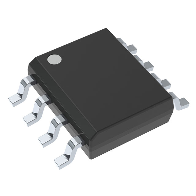
The OP07CDG4 is a General Purpose Operational Amplifier (Op-Amp) designed by Texas Instruments, renowned for its precision and reliability. This Op-Amp is housed in an 8-SOIC package and is ideal for a wide range of applications requiring high precision and low noise. The OP07CDG4 operates over a supply voltage range of 6V to 36V, making it versatile for various power supply configurations. It features a low input bias current of 1.8 nA and an input offset voltage of 60 µV, ensuring high accuracy in signal processing. With a gain bandwidth product of 600 kHz and a slew rate of 0.3V/µs, the OP07CDG4 delivers stable performance across a broad frequency spectrum. The device is RoHS3 compliant and REACH unaffected, adhering to stringent environmental standards. It is available in a tube package and has a moisture sensitivity level (MSL) of 1, making it suitable for surface mount applications without the need for special handling.
OP07CDG4 Features
- Wide Supply Voltage Range: The OP07CDG4 operates from 6V to 36V, offering flexibility in power supply design.
- Low Input Bias Current: With an input bias current of just 1.8 nA, the OP07CDG4 minimizes the loading effect on the input signal source.
- Low Input Offset Voltage: An input offset voltage of 60 µV ensures high accuracy in signal amplification.
- High Gain Bandwidth Product: A gain bandwidth product of 600 kHz allows for stable performance across a broad range of frequencies.
- Surface Mount Compatibility: The OP07CDG4 is designed for surface mount applications, facilitating compact and efficient PCB designs.
- Environmental Compliance: The device is RoHS3 compliant and REACH unaffected, meeting global environmental standards.
- Moisture Sensitivity Level 1: The OP07CDG4 has an MSL of 1, making it suitable for surface mount applications without the need for special handling.
OP07CDG4 Applications
The OP07CDG4 is well-suited for applications requiring high precision and low noise. Its wide supply voltage range and low input bias current make it ideal for:
- Precision Signal Amplification: The low input bias current and offset voltage ensure accurate amplification of weak signals.
- Analog-to-Digital Conversion: The OP07CDG4 can be used as a buffer or gain stage in ADC circuits, enhancing signal integrity.
- Sensor Interface Circuits: Its high precision and low noise characteristics make it suitable for interfacing with sensitive sensors.
- Audio Signal Processing: The wide bandwidth and low distortion make the OP07CDG4 ideal for audio applications.
- Industrial Control Systems: The device's robustness and wide operating temperature range (0°C to 70°C) make it suitable for industrial environments.
Conclusion of OP07CDG4
The OP07CDG4 is a versatile and high-performance General Purpose Op-Amp that excels in precision and reliability. Its wide supply voltage range, low input bias current, and low input offset voltage make it suitable for a variety of applications, from precision signal amplification to industrial control systems. The device's environmental compliance and surface mount compatibility further enhance its appeal for modern electronics design. Whether used in audio processing, sensor interfacing, or ADC circuits, the OP07CDG4 delivers stable and accurate performance, making it a reliable choice for engineers and designers in the electronics industry.
FAQ
Not available to buy online? Want the lower wholesale price? Please Send RFQ to get best price, we will respond immediately


.png?x-oss-process=image/format,webp/resize,h_32)


