
 German
 Japanese
 Portuguese
 Korea
Korea
 Mexico
 Dutch
Dutch


Texas Instruments
OPA145IDBVT

Why Choose Us?
Professional Platform
B2B & B2C purchasingDelivery at full speed
1-2 days deliveryWide variety
Original manufacturers365 days guarantee
Responsible quality
.png)


Tech Specifications
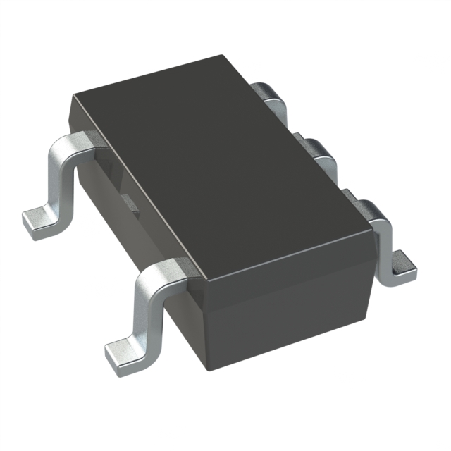
OPA145IDBVT Description
OPA145IDBVT Description
The OPA145IDBVT from Texas Instruments is a high-performance, JFET-input operational amplifier in a compact SOT23-5 package, designed for precision analog applications. With an ultra-low input bias current of 2 pA and a minimal input offset voltage of 40 µV, it ensures exceptional accuracy in signal conditioning. Operating over a wide supply range of 4.5V to 36V, it delivers 5.5 MHz gain bandwidth and a slew rate of 20V/µs, making it suitable for high-speed and low-power designs. Its ROHS3 compliance and REACH unaffected status ensure environmental and regulatory compatibility.
OPA145IDBVT Features
- Ultra-Low Input Bias Current (2 pA): Ideal for high-impedance sensor interfaces and photodiode amplification.
- Low Offset Voltage (40 µV): Enhances precision in DC-coupled applications.
- Wide Supply Range (4.5V–36V): Supports flexible power configurations in industrial and automotive systems.
- High Slew Rate (20V/µs): Enables fast signal response in data acquisition and active filtering.
- Low Quiescent Current (445µA): Optimizes power efficiency in battery-operated devices.
- Stable with Capacitive Loads: Reduces the need for external compensation in challenging layouts.
OPA145IDBVT Applications
The OPA145IDBVT excels in precision instrumentation, medical devices, and test equipment due to its low noise and high accuracy. Its JFET input makes it perfect for pH meters, electrometer amplifiers, and photodiode transimpedance amplifiers. The high slew rate and bandwidth suit active filters, ADC drivers, and audio processing. In industrial systems, it’s used for signal conditioning in PLCs and motor control feedback loops.
Conclusion of OPA145IDBVT
The OPA145IDBVT stands out for its low-power precision, wide voltage range, and robust performance, making it a versatile choice for demanding analog designs. Its small form factor (SOT23-5) and tape & reel packaging streamline high-volume production. Engineers will appreciate its balance of speed, accuracy, and power efficiency, particularly in sensor interfaces, medical electronics, and industrial control systems. For applications requiring high impedance, low noise, and stability, this op-amp is a superior solution.
FAQ
Not available to buy online? Want the lower wholesale price? Please Send RFQ to get best price, we will respond immediately


.png?x-oss-process=image/format,webp/resize,h_32)


