
 German
 Japanese
 Portuguese
 Korea
Korea
 Mexico
 Dutch
Dutch


Texas Instruments
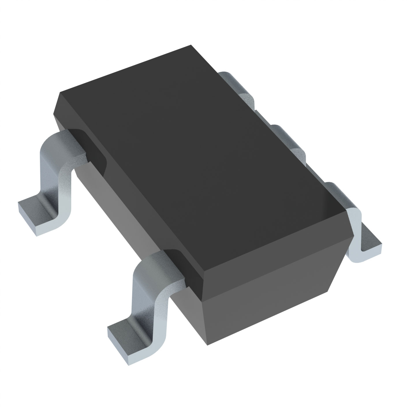
OPA171AQDBVRQ1

Why Choose Us?
Professional Platform
B2B & B2C purchasingDelivery at full speed
1-2 days deliveryWide variety
Original manufacturers365 days guarantee
Responsible quality
.png)


Tech Specifications
OPA171AQDBVRQ1 Description
The Texas Instruments OPA171AQDBVRQ1 is a precision operational amplifier (op-amp) designed for high-accuracy applications. Here is a description of the model, its features, and potential applications:
Description:
The OPA171AQDBVRQ1 is a low-noise, precision operational amplifier offered in a small-outline (SO) 8-pin package. It is designed to provide excellent DC and AC performance, making it suitable for a wide range of applications that require high precision and low noise.
Features:
-
Low Input Offset Voltage: The OPA171AQDBVRQ1 has an input offset voltage as low as 100µV (typical), which is crucial for maintaining accuracy in precision applications.
-
Low Input Bias Current: With an input bias current of typically 1pA, this op-amp is ideal for driving high-impedance loads without introducing significant errors.
-
Low Noise: The OPA171AQDBVRQ1 features a low noise level of 4.5nV/√Hz, making it suitable for applications where signal-to-noise ratio is critical.
-
High Slew Rate: A slew rate of 7V/µs allows the op-amp to respond quickly to fast-changing input signals.
-
Wide Supply Voltage Range: The device can operate with supply voltages from ±2.5V to ±18V, providing flexibility in system design.
-
Low Output Drift: The output voltage drift is minimal over a wide temperature range, ensuring stable performance in varying environmental conditions.
-
Short-Circuit Protection: The OPA171AQDBVRQ1 includes internal protection against short circuits, which can help prevent damage to the device under fault conditions.
-
Low Power Consumption: The device consumes a low quiescent current, making it suitable for battery-powered and energy-sensitive applications.
Applications:
-
Data Acquisition Systems: The OPA171AQDBVRQ1's low noise and high precision make it ideal for use in data acquisition systems where accurate signal processing is required.
-
Medical Instruments: In medical equipment, precision and low noise are critical, and this op-amp can be used in signal conditioning circuits for ECG machines, blood pressure monitors, and other diagnostic devices.
-
Sensor Conditioning: The low drift and low noise characteristics of the OPA171AQDBVRQ1 make it suitable for conditioning signals from sensors in industrial control systems.
-
Audio Equipment: For high-fidelity audio applications, the low noise and high accuracy of this op-amp can be used in preamplifiers and other audio processing circuits.
-
Strain Gauge Amplification: In applications involving strain gauges for force or pressure measurement, the OPA171AQDBVRQ1 can provide the necessary precision and stability.
-
Temperature Measurement: For systems that require precise temperature measurements, such as in climate control or industrial process control, this op-amp can be used to condition signals from temperature sensors.
-
Battery Monitors: In battery monitoring systems, the low power consumption and high accuracy of the OPA171AQDBVRQ1 can help maintain long battery life while providing precise voltage and current measurements.
The OPA171AQDBVRQ1 is a versatile and high-performance operational amplifier that can be integrated into a wide range of precision electronic systems where low noise, high accuracy, and stability are paramount.
FAQ
| Quantity | Unit Price | Ext. Price |
|---|---|---|
| 1+ | $1.26515 | $1.27 |
| 10+ | $1.06115 | $10.61 |
| 30+ | $0.94972 | $28.49 |
Not available to buy online? Want the lower wholesale price? Please Send RFQ to get best price, we will respond immediately


.png?x-oss-process=image/format,webp/resize,h_32)


