
 German
 Japanese
 Portuguese
 Korea
Korea
 Mexico
 Dutch
Dutch


Texas Instruments
OPA202IDGKT
687-OPA202IDGKT

PDF Datasheet
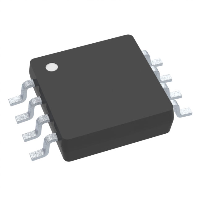
Precision Op Amp, Low Noise, 1000MHz, 8-Pin VSSOP
6 Weeks
Why Choose Us?
Professional Platform
B2B & B2C purchasingDelivery at full speed
1-2 days deliveryWide variety
Original manufacturers365 days guarantee
Responsible quality
.png)


Tech Specifications
Max Operating Temperature
105
Number of Terminals
8
Min Operating Temperature
-40
Terminal Position
DUAL
JEDEC Package Code
S-PDSO-G8
Width
3
Length
3
Number of Functions
1
OPA202IDGKT Description
General Purpose Amplifier 1 Circuit Push-Pull 8-VSSOP
FAQ
Are there related or alternative parts for OPA202IDGKT?
Yes. Related or alternative parts may be available on this page when relevant product data is provided.
What operating temperature range does OPA202IDGKT support?
What package or case is OPA202IDGKT available in?
What is OPA202IDGKT?
What is the standard lead time for OPA202IDGKT?
Quick Quote
ADD TO RFQ LIST
Not available to buy online? Want the lower wholesale price? Please Send RFQ to get best price, we will respond immediately
QUICK RFQ


.png?x-oss-process=image/format,webp/resize,h_32)


