

Texas Instruments
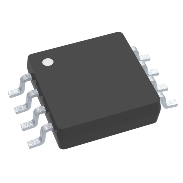
OPA211AIDGKTG4
OP Amps, Buffer Amps ICs

Not available to buy online? Want the lower wholesale price? Please Send RFQ to get best price, we will respond immediately


.png?x-oss-process=image/format,webp/resize,p_30)


OPA211AIDGKTG4 Description
OPA211AIDGKTG4 Description
The OPA211AIDGKTG4 is a high-performance general-purpose operational amplifier (op-amp) from Texas Instruments, designed for a wide range of analog signal processing applications. This op-amp is housed in an 8-pin VSSOP package, making it suitable for surface-mount applications where space is at a premium. The OPA211AIDGKTG4 offers a wide supply voltage range, from 4.5 V to 36 V, ensuring compatibility with various power supply configurations. It features a gain bandwidth product of 80 MHz, enabling high-frequency signal processing with minimal distortion. The op-amp's input bias current is a low 60 nA, which is ideal for high-impedance applications. Additionally, it has a low input offset voltage of 30 µV, ensuring accurate signal amplification. The OPA211AIDGKTG4 also boasts a high slew rate of 27 V/µs, allowing it to handle fast-changing signals effectively. It is REACH unaffected and RoHS3 compliant, making it suitable for environmentally conscious designs. The op-amp has a supply current of 3.6 mA and can source or sink up to 30 mA per channel, making it suitable for driving moderate loads. The moisture sensitivity level (MSL) is 2 (1 year), ensuring reliability in various environmental conditions. The OPA211AIDGKTG4 is classified under ECCN EAR99 and HTSUS 8542.33.0001, and it is available in tape and reel packaging for bulk handling and automated assembly processes.
OPA211AIDGKTG4 Features
- Wide Supply Voltage Range: Operates from 4.5 V to 36 V, providing flexibility in power supply requirements.
- High Gain Bandwidth Product: 80 MHz, enabling high-frequency signal processing with minimal distortion.
- Low Input Bias Current: 60 nA, ideal for high-impedance applications.
- Low Input Offset Voltage: 30 µV, ensuring accurate signal amplification.
- High Slew Rate: 27 V/µs, allowing for the handling of fast-changing signals.
- Low Supply Current: 3.6 mA, contributing to energy-efficient designs.
- High Output Current: 30 mA per channel, capable of driving moderate loads.
- Environmental Compliance: REACH unaffected and RoHS3 compliant, suitable for environmentally conscious designs.
- Reliability: MSL 2 (1 year), ensuring reliability in various environmental conditions.
- Packaging: Available in tape and reel (TR) for bulk handling and automated assembly processes.
OPA211AIDGKTG4 Applications
The OPA211AIDGKTG4 is ideal for a variety of applications due to its versatile performance characteristics. It is particularly well-suited for:
- Analog Signal Processing: Amplifying and conditioning signals in audio, instrumentation, and industrial control systems.
- High-Frequency Applications: Its 80 MHz gain bandwidth product makes it suitable for high-frequency signal processing in communication and radar systems.
- High-Impedance Applications: The low input bias current of 60 nA is beneficial for applications requiring high input impedance, such as photodetector circuits.
- Precision Amplification: The low input offset voltage of 30 µV ensures accurate amplification in precision measurement and control systems.
- Power-Efficient Designs: The low supply current of 3.6 mA is advantageous in battery-powered and energy-efficient applications.
- Moderate Load Driving: The ability to source or sink 30 mA per channel makes it suitable for driving moderate loads in various electronic systems.
Conclusion of OPA211AIDGKTG4
The OPA211AIDGKTG4 operational amplifier from Texas Instruments is a versatile and high-performance solution for a wide range of analog signal processing applications. Its wide supply voltage range, high gain bandwidth product, low input bias current, and low input offset voltage make it suitable for high-impedance and precision amplification tasks. The high slew rate ensures effective handling of fast-changing signals, while the low supply current and high output current capability make it ideal for power-efficient and moderate load driving applications. The OPA211AIDGKTG4's environmental compliance and reliability further enhance its suitability for modern, environmentally conscious designs. Whether used in audio systems, industrial controls, or high-frequency communication systems, the OPA211AIDGKTG4 offers a robust and reliable solution for engineers and designers in the electronics industry.
Tech Specifications
OPA211AIDGKTG4 Documents
Download datasheets and manufacturer documentation for OPA211AIDGKTG4
Mechanical Outline Drawing Function Diagram Process Change Notification (PDF) TI - PCN - 8-5-10 (PDF) Product Change Notification (PDF) OPA211AIDGKTG4 Symbol & Footprint by SnapMagic Design and analysis of a TGC circuit to drive the control voltage OPA211 OPA211A OP2211 OPA2211A EMI Immunity Performance Operational amplifier gain stability Part 3: AC gain-error analysis 3Q 2010 Issue Analog Applications Journal Operational amplifier gain stability Part 2: DC gain-error analysis 2Q 2010 Issue Analog Applications Journal DAC force and sense reference drive circuit Using infinite-gain MFB filter topology in fully differential active filters OPA211 TINA-TI Reference Design (Rev. F) OPA211 TINA-TI Reference Design (Rev. D) OPA211 TINA-TI Reference Design (Rev. E) OPA211 PSpice Model (Rev. C) OPA211 TINA-TI Spice Model (Rev. C) OPA211 TINA-TI Spice Model (Rev. E) OPA211 PSpice Model (Rev. A) Related Parts


Shopping Guide


.png?x-oss-process=image/format,webp/resize,h_32)


©2025 ERSA Electronics Corporation.