
 German
 Japanese
 Portuguese
 Korea
Korea
 Mexico
 Dutch
Dutch


Texas Instruments
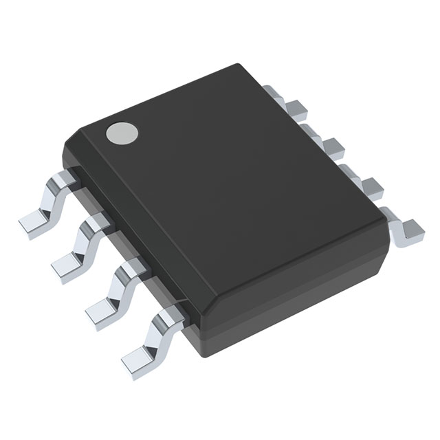
OPA2192ID

Why Choose Us?
Professional Platform
B2B & B2C purchasingDelivery at full speed
1-2 days deliveryWide variety
Original manufacturers365 days guarantee
Responsible quality
.png)


Tech Specifications
OPA2192ID Description
OPA2192ID Description
The OPA2192ID is a high-performance operational amplifier from Texas Instruments, designed for a wide range of general-purpose applications. This dual-channel op-amp is part of the MicroAmplifier™ series and is housed in a surface-mount package, making it suitable for compact and high-density PCB designs. The OPA2192ID operates over a wide supply voltage range, from 4.5 V to 36 V, and offers a gain bandwidth product of 10 MHz, ensuring excellent performance in various analog signal processing tasks.
OPA2192ID Features
- Wide Supply Voltage Range: The OPA2192ID can operate with a supply voltage spanning from 4.5 V to 36 V, making it versatile for different power supply configurations.
- Low Input Bias Current: With an input bias current of just 5 pA, the OPA2192ID minimizes the loading effect on high-impedance sources, ensuring accurate signal amplification.
- High Slew Rate: The 20 V/µs slew rate allows the OPA2192ID to handle high-frequency signals with minimal distortion, making it suitable for applications requiring fast transient response.
- Low Input Offset Voltage: The 5 µV input offset voltage ensures high precision in signal amplification, which is crucial for applications where accuracy is paramount.
- High Output Current: Each channel can deliver up to 65 mA, enabling the OPA2192ID to drive moderate to high load currents effectively.
- Compliance and Reliability: The OPA2192ID is REACH unaffected and RoHS3 compliant, ensuring it meets environmental and safety standards. It also has a moisture sensitivity level (MSL) of 2, which allows for a 1-year shelf life under standard conditions.
OPA2192ID Applications
The OPA2192ID is ideal for a variety of applications due to its combination of high performance and versatility. Some specific use cases include:
- Precision Signal Conditioning: The low input bias current and low input offset voltage make the OPA2192ID suitable for precision instrumentation and measurement applications where high accuracy is required.
- Audio Amplification: The high slew rate and wide bandwidth enable the OPA2192ID to handle audio signals with minimal distortion, making it ideal for high-fidelity audio systems.
- Industrial Control Systems: The wide supply voltage range and high output current capability allow the OPA2192ID to be used in industrial control systems where robustness and reliability are critical.
- Medical Equipment: The high precision and low noise characteristics of the OPA2192ID make it suitable for medical devices that require accurate signal processing.
Conclusion of OPA2192ID
The OPA2192ID from Texas Instruments is a versatile and high-performance operational amplifier that stands out in its class. Its wide supply voltage range, low input bias current, high slew rate, and low input offset voltage make it suitable for a wide range of applications, from precision signal conditioning to high-fidelity audio systems. The OPA2192ID's compliance with environmental and safety standards, along with its reliability, further enhances its appeal for use in various industries. Whether in industrial control systems or medical equipment, the OPA2192ID delivers the performance and reliability needed to meet the demands of modern electronics.
FAQ
Not available to buy online? Want the lower wholesale price? Please Send RFQ to get best price, we will respond immediately


.png?x-oss-process=image/format,webp/resize,h_32)


