
Texas Instruments
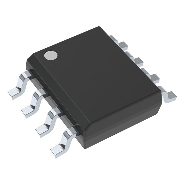
OPA2206ADR
OP Amps, Buffer Amps ICs


.png?x-oss-process=image/format,webp/resize,p_30)


OPA2206ADR Description
OPA2206ADR Description
The OPA2206ADR is a high-performance, dual-channel, general-purpose operational amplifier from Texas Instruments, designed to deliver exceptional performance in a wide range of applications. This op-amp features a wide supply voltage range, from 4.5 V to 36 V, making it suitable for both low-voltage and high-voltage systems. With a supply current of only 220 µA per channel, the OPA2206ADR is optimized for low-power consumption, which is crucial for battery-powered and energy-efficient designs.
The OPA2206ADR boasts a slew rate of 4 V/µs and a gain bandwidth product of 3.6 MHz, ensuring fast response times and high-frequency performance. Its low input bias current of 100 pA and low input offset voltage of 4 µV contribute to high precision and stability in signal processing applications. The amplifier can deliver up to 25 mA of output current per channel, providing robust drive capabilities for various loads.
OPA2206ADR Features
- Wide Supply Voltage Range: Operates from 4.5 V to 36 V, offering flexibility in power supply requirements.
- Low-Power Consumption: Each channel consumes only 220 µA, making it ideal for low-power applications.
- High Slew Rate: 4 V/µs ensures fast transient response, suitable for high-speed signal processing.
- High Gain Bandwidth Product: 3.6 MHz allows for high-frequency operation and wide bandwidth applications.
- Low Input Bias Current: 100 pA minimizes input loading effects, enhancing precision in sensor interfaces.
- Low Input Offset Voltage: 4 µV ensures high accuracy in signal conditioning and measurement circuits.
- High Output Current: 25 mA per channel provides strong drive capabilities for various loads.
- Surface Mount Package: Tape & Reel (TR) packaging facilitates easy integration into surface-mount designs.
- Compliance and Reliability: REACH unaffected and RoHS3 compliant, ensuring environmental and regulatory standards are met.
- Moisture Sensitivity Level: MSL 2 (1 Year) ensures reliability in manufacturing processes.
OPA2206ADR Applications
The OPA2206ADR is well-suited for a variety of applications due to its versatile performance characteristics. It is ideal for precision signal conditioning in instrumentation and measurement systems, where low noise and high accuracy are critical. Its wide supply voltage range and low power consumption make it suitable for portable and battery-powered devices, such as handheld instruments and medical equipment.
In industrial automation, the OPA2206ADR can be used in sensor signal processing, providing high precision and stability. Its high slew rate and bandwidth make it suitable for high-speed data acquisition systems and communication interfaces. Additionally, its robust output current capability allows it to drive various types of loads, including transducers and actuators.
Conclusion of OPA2206ADR
The OPA2206ADR from Texas Instruments is a versatile and high-performance dual-channel operational amplifier that offers a combination of wide supply voltage range, low power consumption, and high precision. Its low input bias current and low input offset voltage make it ideal for precision applications, while its high slew rate and bandwidth ensure fast and accurate signal processing. The OPA2206ADR's surface mount package and compliance with environmental and regulatory standards further enhance its suitability for modern electronic designs. Whether in precision instrumentation, industrial automation, or portable devices, the OPA2206ADR provides reliable and efficient performance, making it a preferred choice for engineers and designers in the electronics industry.
Tech Specifications
OPA2206ADR Documents
Download datasheets and manufacturer documentation for OPA2206ADR
 OPAx206
 Shopping Guide


.png?x-oss-process=image/format,webp/resize,h_32)


