
 German
 Japanese
 Portuguese
 Korea
Korea
 Mexico
 Dutch
Dutch


Texas Instruments
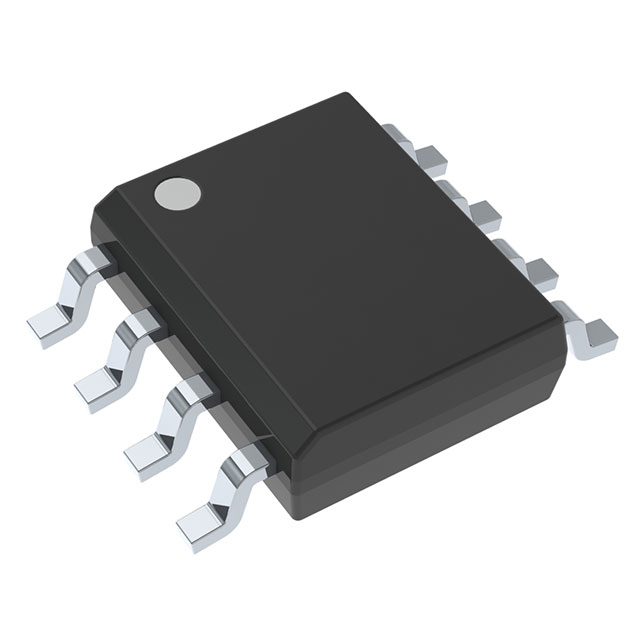
OPA2209AID

Why Choose Us?
Professional Platform
B2B & B2C purchasingDelivery at full speed
1-2 days deliveryWide variety
Original manufacturers365 days guarantee
Responsible quality
.png)


Tech Specifications
OPA2209AID Description
The OPA2209AID is a precision operational amplifier (op-amp) from Texas Instruments. It is designed for high-precision applications and offers excellent performance in terms of input offset voltage, drift, and noise.
Description:
The OPA2209AID is a low-power, precision operational amplifier that is available in an 8-pin DIP (dual in-line package) or SOIC (small-outline integrated circuit) package. It features a wide supply voltage range of 3V to 36V and offers low input offset voltage and drift, making it ideal for a variety of precision applications.
Features:
- Low input offset voltage: 1µV maximum
- Low input bias current: 1pA maximum
- Low drift: 0.05µV/°C typical
- Wide supply voltage range: 3V to 36V
- Low noise: 5nV/√Hz typical
- High output current: ±35mA
- Rail-to-rail input and output
Applications:
The OPA2209AID is suitable for a wide range of precision applications, including:
- Strain gauge amplifiers
- pH meter amplifiers
- Pressure sensor amplifiers
- Weighing applications
- Medical instrumentation
- Data acquisition systems
- Precision filtering and buffering
- Battery monitoring systems
Overall, the OPA2209AID is a high-performance operational amplifier that offers excellent precision and low power consumption, making it an ideal choice for a variety of applications where accuracy and stability are critical.
FAQ
Not available to buy online? Want the lower wholesale price? Please Send RFQ to get best price, we will respond immediately


.png?x-oss-process=image/format,webp/resize,h_32)


