

Texas Instruments
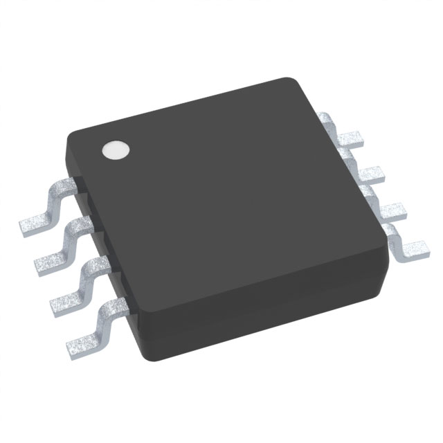
OPA2330AIDGKT
OP Amps, Buffer Amps ICs

Not available to buy online? Want the lower wholesale price? Please Send RFQ to get best price, we will respond immediately


.png?x-oss-process=image/format,webp/resize,p_30)


OPA2330AIDGKT Description
OPA2330AIDGKT Description
The OPA2330AIDGKT is a high-performance, zero-drift operational amplifier from Texas Instruments, designed for precision signal conditioning in a wide range of applications. This dual-channel op-amp features an 8-VSSOP package, making it suitable for surface-mount applications where space is a critical consideration. The OPA2330AIDGKT operates over a wide supply voltage range, from 1.8 V to 5.5 V, ensuring compatibility with various power supply configurations. Each channel of the OPA2330AIDGKT draws a low supply current of 21 µA, contributing to its energy-efficient operation.
OPA2330AIDGKT Features
- Zero-Drift Technology: The OPA2330AIDGKT employs zero-drift technology, which ensures minimal offset voltage drift over time and temperature, making it ideal for precision applications.
- Wide Supply Voltage Range: With a supply voltage range of 1.8 V to 5.5 V, the OPA2330AIDGKT is versatile and can be used in systems with varying power supply requirements.
- Low Input Bias Current: The low input bias current of 200 pA ensures that the op-amp does not significantly load the input signal source, preserving signal integrity.
- High Gain Bandwidth Product: A gain bandwidth product of 350 kHz allows for high-frequency signal processing, making the OPA2330AIDGKT suitable for applications requiring wide bandwidth.
- Low Slew Rate: The 0.16 V/µs slew rate ensures stable performance and minimal distortion in signal amplification.
- Low Voltage Input Offset: The low input offset voltage of 8 µV ensures high accuracy in signal processing, crucial for precision applications.
- High Output Current: Each channel can deliver up to 5 mA of output current, enabling the op-amp to drive moderate loads effectively.
- Compliance and Reliability: The OPA2330AIDGKT is REACH unaffected and RoHS3 compliant, ensuring environmental sustainability and regulatory compliance. It also has a moisture sensitivity level (MSL) of 1, making it suitable for unlimited storage conditions.
OPA2330AIDGKT Applications
The OPA2330AIDGKT is well-suited for applications requiring high precision and low power consumption. Its zero-drift technology and low input bias current make it ideal for:
- Precision Signal Conditioning: In sensor interfaces and transducers, where accurate signal amplification and conditioning are essential.
- Low-Power Systems: Suitable for battery-powered devices and portable electronics due to its low supply current.
- Medical Equipment: Ideal for medical devices requiring high precision and reliability, such as ECG and EEG machines.
- Industrial Control Systems: Used in industrial automation and control systems where precise signal processing and low noise are critical.
- Data Acquisition Systems: Effective in data acquisition systems where accurate signal amplification and minimal drift are required.
Conclusion of OPA2330AIDGKT
The OPA2330AIDGKT from Texas Instruments is a robust and versatile operational amplifier that offers exceptional performance in precision signal processing applications. Its zero-drift technology, wide supply voltage range, and low power consumption make it a standout choice for designers seeking high accuracy and reliability. The OPA2330AIDGKT's compliance with environmental and regulatory standards further enhances its appeal for modern electronics applications. Whether used in medical devices, industrial control systems, or portable electronics, the OPA2330AIDGKT delivers reliable performance and precision, making it a valuable component in any high-performance design.
Tech Specifications
OPA2330AIDGKT Documents
Download datasheets and manufacturer documentation for OPA2330AIDGKT
Mechanical Outline Drawing Function Diagram Conversion to Cu Wire for Selected Devices (PDF) Product Change Notification (PDF) OPA2317/2330/2333, OPA317/330/333, TLV2333/333 Product Family Die Enhancement (PDF) OPA2330AIDGKT Symbol & Footprint by SnapMagic OPA330 TINA-TI Reference Design (Rev. B) OPA330 TINA-TI Reference Design (Rev. C) OPA2330 TINA-TI Reference Design OPA2330 PSPICE Model OPA330 TINA-TI Spice Model (Rev. C) OPA330 TINA-TI Spice Model (Rev. B) OPA330 PSpice Model (Rev. D) OPA2330 TINA-TI Spice Model OPA330 PSpice Model (Rev. C) Related Parts


Shopping Guide


.png?x-oss-process=image/format,webp/resize,h_32)


©2025 ERSA Electronics Corporation.