
Texas Instruments
OPA2333AID
OP Amps, Buffer Amps ICs


.png?x-oss-process=image/format,webp/resize,p_30)


OPA2333AID Description
OPA2333AID Description
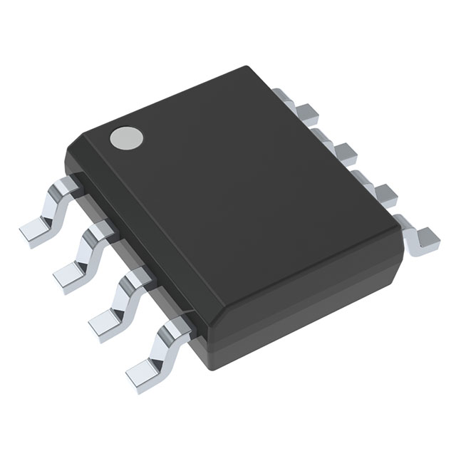
The OPA2333AID is a high-performance, zero-drift operational amplifier from Texas Instruments, designed to deliver exceptional performance in precision analog applications. This dual-channel op-amp is housed in an 8-pin SOIC package, making it suitable for surface-mount applications where space is a premium. The OPA2333AID offers a wide supply voltage range, from 1.8 V to 5.5 V, ensuring compatibility with a variety of power supply configurations. Its low input bias current of 70 pA and an ultra-low input offset voltage of 2 µV make it ideal for high-precision signal conditioning tasks.
OPA2333AID Features
- Wide Supply Voltage Range: The OPA2333AID operates from a supply voltage range of 1.8 V to 5.5 V, providing flexibility in power supply design.
- Low Input Bias Current: With an input bias current of just 70 pA, the OPA2333AID minimizes the effects of input current on the signal source, ensuring high accuracy in precision applications.
- Ultra-Low Input Offset Voltage: The 2 µV input offset voltage ensures minimal error in the output signal, making it suitable for applications requiring high precision.
- Zero-Drift Architecture: The zero-drift design eliminates long-term drift and 1/f noise, ensuring stable performance over time and across temperature variations.
- Low Supply Current: Each channel of the OPA2333AID consumes only 17 µA, making it energy-efficient for battery-powered and low-power applications.
- High Slew Rate: The 0.16 V/µs slew rate ensures fast response times, making it suitable for applications requiring high-speed signal processing.
- High Output Current: Each channel can deliver up to 5 mA, providing robust performance in driving loads.
- Compliance and Reliability: The OPA2333AID is REACH unaffected and RoHS3 compliant, ensuring environmental and regulatory compliance. It also has a moisture sensitivity level (MSL) of 1, making it suitable for unlimited storage and handling.
OPA2333AID Applications
The OPA2333AID is ideal for a wide range of applications that demand high precision and low noise. Some specific use cases include:
- Precision Signal Conditioning: Ideal for applications such as sensor interfaces, where high accuracy and low noise are critical.
- Battery-Powered Devices: The low supply current makes it suitable for portable and battery-powered applications, ensuring long battery life.
- Medical Equipment: The zero-drift architecture and low offset voltage make it suitable for medical devices that require high precision and stability.
- Industrial Control Systems: The wide supply voltage range and robust performance make it suitable for industrial applications where reliability and precision are paramount.
- Data Acquisition Systems: The low noise and high slew rate make it suitable for data acquisition systems requiring high-speed and high-precision signal processing.
Conclusion of OPA2333AID
The OPA2333AID from Texas Instruments is a versatile and high-performance operational amplifier that offers exceptional precision and stability. Its wide supply voltage range, low input bias current, and ultra-low input offset voltage make it suitable for a variety of precision applications. The zero-drift architecture ensures long-term stability and minimal drift, making it an ideal choice for applications where high accuracy and reliability are essential. Whether used in precision signal conditioning, battery-powered devices, or industrial control systems, the OPA2333AID delivers outstanding performance and reliability.
Tech Specifications
OPA2333AID Documents
Download datasheets and manufacturer documentation for OPA2333AID
 OPA333, OPA2333
  OPA333, OPA2333
  Design 25/Feb/2022 Mult Dev 27/Jul/2023
 Shopping Guide


.png?x-oss-process=image/format,webp/resize,h_32)


