
Texas Instruments
OPA2364IDR
OP Amps, Buffer Amps ICs


.png?x-oss-process=image/format,webp/resize,p_30)


OPA2364IDR Description
OPA2364IDR Description
The OPA2364IDR is a high-performance, dual CMOS operational amplifier from Texas Instruments. It boasts an impressive gain bandwidth product of 7 MHz and a slew rate of 5V/µs, making it ideal for high-speed applications. With a supply voltage range of 1.8 V to 5.5 V, it offers flexibility in power supply design. The device is compliant with the RoHS3 directive and is unaffected by REACH regulations, ensuring environmental compliance.
OPA2364IDR Features
- Low Input Bias Current: The OPA2364IDR has an ultra-low input bias current of 1 pA, which is crucial for applications requiring high input impedance, such as sensor interfaces.
- Low Voltage Operation: With a minimum supply voltage of 1.8 V, the OPA2364IDR is suitable for low-voltage systems, extending battery life in portable devices.
- High Slew Rate: The 5V/µs slew rate allows for fast response times, making it suitable for high-speed signal processing.
- Dual Channel: The OPA2364IDR features two independent operational amplifiers in a single package, saving space and reducing component count in dual-channel applications.
- Low Input Offset Voltage: The 900 µV input offset voltage ensures high accuracy in applications requiring precise amplification.
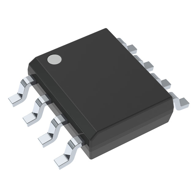
- Surface Mount Packaging: The device is available in an 8-SOIC package, suitable for surface-mount applications, reducing footprint and improving manufacturing efficiency.
OPA2364IDR Applications
The OPA2364IDR is ideal for a variety of applications due to its high performance and low power consumption:
- Audio Amplification: Its low noise and high slew rate make it suitable for audio applications, such as headphone amplifiers and preamplifiers.
- Sensor Interfaces: The low input bias current and low offset voltage are beneficial for accurate sensor signal conditioning in industrial and medical applications.
- Data Acquisition Systems: The high gain bandwidth product and low noise make it suitable for high-speed data acquisition systems in test and measurement equipment.
- Communication Systems: The OPA2364IDR can be used in communication systems for signal conditioning and amplification of high-frequency signals.
Conclusion of OPA2364IDR
The OPA2364IDR is a versatile, high-performance dual operational amplifier that offers a combination of low power consumption, high speed, and precision. Its unique features, such as low input bias current and low voltage operation, make it an excellent choice for a wide range of applications, from audio amplification to sensor interfaces and data acquisition systems. With its compliance with environmental regulations and space-saving dual-channel design, the OPA2364IDR is a reliable and efficient solution for high-speed, low-voltage applications.
Tech Specifications
OPA2364IDR Documents
Download datasheets and manufacturer documentation for OPA2364IDR
 Fab Site Addition 13/Mar/2015
  OPA4364AIDG4
  Design 25/Feb/2022
 Shopping Guide


.png?x-oss-process=image/format,webp/resize,h_32)


