
 German
 Japanese
 Portuguese
 Korea
Korea
 Mexico
 Dutch
Dutch


Texas Instruments
OPA2387DSGT

Why Choose Us?
Professional Platform
B2B & B2C purchasingDelivery at full speed
1-2 days deliveryWide variety
Original manufacturers365 days guarantee
Responsible quality
.png)


Tech Specifications
OPA2387DSGT Description
OPA2387DSGT Description
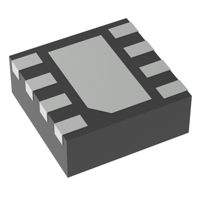
The OPA2387DSGT is an ultra-high precision, zero-drift operational amplifier designed by Texas Instruments. This dual-channel device is optimized for applications requiring exceptional accuracy and stability. With a supply voltage range of 1.7 V to 5.5 V, it offers flexibility in power supply design. The OPA2387DSGT features a gain bandwidth product of 5.7 MHz and a slew rate of 2.8 V/µs, ensuring high-performance signal processing. Each channel consumes only 570 µA, making it suitable for low-power applications. The device is housed in a surface-mount package, specifically Tape & Reel (TR), which is ideal for automated assembly processes.
OPA2387DSGT Features
- Ultra-High Precision and Zero-Drift: The OPA2387DSGT is designed to maintain high precision over time and temperature, making it ideal for applications where accuracy is critical.
- Wide Supply Voltage Range: With a supply voltage range from 1.7 V to 5.5 V, the OPA2387DSGT can operate in a variety of power supply environments.
- Low Input Bias Current: The input bias current of 30 pA ensures minimal loading effects on the signal source, which is crucial for high-impedance applications.
- Low Input Offset Voltage: The low input offset voltage of 0.25 µV guarantees accurate signal amplification, even at low signal levels.
- High Output Current: Each channel can deliver up to 55 mA, enabling the amplifier to drive heavy loads effectively.
- Surface-Mount Packaging: The surface-mount package (Tape & Reel) facilitates easy integration into modern PCB designs and supports high-volume manufacturing.
- Compliance and Reliability: The OPA2387DSGT is REACH unaffected and RoHS3 compliant, ensuring environmental and regulatory compliance. It also has a moisture sensitivity level (MSL) of 1, making it suitable for unlimited storage conditions.
OPA2387DSGT Applications
The OPA2387DSGT is ideal for applications that demand high precision and stability, such as:
- Precision Signal Conditioning: In industrial and medical equipment, where accurate signal amplification and conditioning are necessary.
- Sensor Interfaces: For interfacing with high-impedance sensors, ensuring minimal signal distortion and high accuracy.
- Low-Power Systems: Suitable for battery-powered devices and portable electronics due to its low power consumption.
- Automotive Electronics: Ideal for automotive applications where reliability and precision are paramount.
- Data Acquisition Systems: In systems requiring high-fidelity signal processing and low noise performance.
Conclusion of OPA2387DSGT
The OPA2387DSGT from Texas Instruments stands out as a superior choice for applications requiring ultra-high precision and zero-drift performance. Its wide supply voltage range, low input bias current, and low input offset voltage make it highly versatile and accurate. The device's low power consumption and high output current capability further enhance its suitability for a wide range of applications. With its surface-mount packaging and compliance with environmental and regulatory standards, the OPA2387DSGT ensures ease of integration and reliability in modern electronic designs.
FAQ
Not available to buy online? Want the lower wholesale price? Please Send RFQ to get best price, we will respond immediately


.png?x-oss-process=image/format,webp/resize,h_32)


