Texas Instruments_OPA2388IDGKR

Texas Instruments
OPA2388IDGKR  
OP Amps, Buffer Amps ICs

Texas Instruments
OPA2388IDGKR
687-OPA2388IDGKR
Ersa
Texas Instruments-OPA2388IDGKR-datasheets-3033916.pdf
IC OPAMP ZER-DRIFT 2CIRC 8VSSOP
In Stock : 2707

Not available to buy online? Want the lower wholesale price? Please Send RFQ to get best price, we will respond immediately

QUICK RFQ
ADD TO RFQ LIST
ersa FreeSample ersa flow
ISO9001
Quality Policy
ISO45001
ISO14001

OPA2388IDGKR Description

The Texas Instruments OPA2388IDGKR is a high-performance, low-noise, dual operational amplifier (op-amp) designed for a wide range of applications. Here's a brief description, features, and applications of the OPA2388IDGKR:

Description:

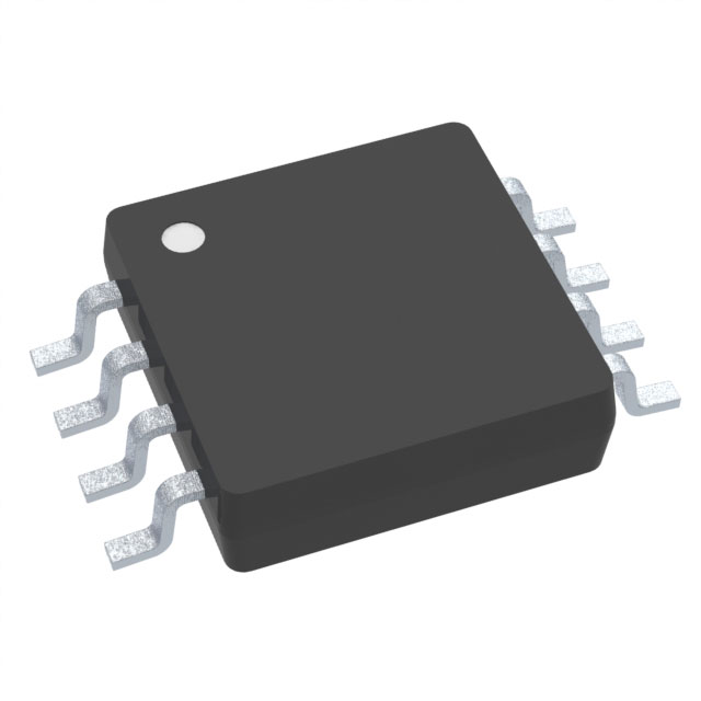
The OPA2388IDGKR is a precision, dual operational amplifier offered in a 8-lead SOIC (SO-8) package. It is designed to provide excellent overall performance, with low input voltage and current noise, low distortion, and high output drive capabilities.

Features:

  1. Low input voltage noise: 4 nV/√Hz at 1 kHz
  2. Low input current noise: 0.8 pA/√Hz at 1 kHz
  3. Low distortion: -90 dBc at 1 kHz (typical)
  4. High output current drive: ±35 mA
  5. Wide supply voltage range: ±2.5V to ±18V
  6. Unity-gain stable with a large range of capacitive loads
  7. Well-suited for both inverting and non-inverting amplifier configurations
  8. Internal frequency compensation
  9. Short-circuit protection
  10. Available in an 8-lead SOIC package

Applications:

  1. Audio preamplifiers and line drivers
  2. Medical instrumentation amplifiers
  3. Strain gauge amplifiers
  4. Precision DC and AC amplifiers
  5. Battery monitors and protection circuits
  6. Photodiode amplifiers
  7. Chemical sensors and pH meters
  8. High-speed data acquisition systems
  9. Precision instrumentation and control systems
  10. Any application requiring low-noise, low-distortion amplification

The OPA2388IDGKR is an excellent choice for applications where low-noise performance, high output drive, and a wide supply voltage range are critical. Its versatility makes it suitable for a wide range of precision amplification tasks in various industries, including audio, medical, industrial, and scientific instrumentation.

Tech Specifications

Number of Channels per Chip
Unit Weight
Power Supply Type
Rail-to-rail
Product
PPAP
Gain Bandwidth Product
Automotive
Maximum Input Offset Current (uA)
RoHS
THD plus Noise
REACH Status
Input common mode headroom (to negative supply) (typ) (V)
Operating temperature range (°C)
Supplier Temperature Grade
Current - Supply
Output swing headroom (to negative supply) (typ) (V)
Standard Package Name
Shut Down Support
Mounting
Minimum Single Supply Voltage (V)
Iout (typ) (A)
Moisture Sensitive
Manufacturer Type
Package
Minimum CMRR (dB)
Total supply voltage (+5 V = 5, ±5 V = 10) (max) (V)
GBW (typ) (MHz)
3 dB Bandwidth
en - Input Voltage Noise Density
Output Type
Vos - Input Offset Voltage
Minimum Dual Supply Voltage
Minimum CMRR Range (dB)
Typical Gain Bandwidth Product (MHz)
Development Kit
Package Height
Maximum Operating Temperature
Ib - Input Bias Current
RoHS Status
Number of channels
Iq per channel (typ) (mA)
Minimum Operating Temperature
Voltage - Input Offset
Type
Vos (offset voltage at 25°C) (max) (mV)
Output Current per Channel
Part Status
Lead finish / Ball material
Number of Circuits
Package Width
GBP - Gain Bandwidth Product
Voltage - Supply Span (Max)
Maximum Input Offset Voltage (mV)
Product Status
Current - Input Bias
Rail to Rail
Supplier Package
Package / Case
Number of Channels
Typical Voltage Gain (dB)
Typical Input Bias Current (uA)
EU RoHS
Carrier
Amplifier Type
Maximum Dual Supply Voltage (V)
Input common mode headroom (to positive supply) (typ) (V)
Moisture Sensitivity Level (MSL)
Typical Input Noise Voltage Density (nV/rtHz)
Operating Temperature
Architecture
Typical Slew Rate (V/us)
Output swing headroom (to positive supply) (typ) (V)
ECCN
MSL rating / Peak reflow
Mounting Type
THD + N at 1 kHz (typ) (%)
Pin Count
In - Input Noise Current Density
Ios - Input Offset Current
Minimum PSRR (dB)
Shutdown
Voltage - Supply Span (Min)
Lead Shape
HTSUS
Pins
Current - Output / Channel
USHTS
Maximum Dual Supply Voltage
PCB changed
HTS
Rating
ECCN (US)
Total supply voltage (+5 V = 5, ±5 V = 10) (min) (V)
Supplier Device Package
Supply Voltage - Min
Minimum Operating Temperature (°C)
Maximum Operating Temperature (°C)
Operating Supply Current
SR - Slew Rate
Mfr
Features
CMRR (typ) (dB)
Supply Voltage - Max
Offset drift (typ) (µV/°C)
Mounting Style
Input Type
Maximum Input Bias Current (uA)
Typical Noninverting Input Current Noise Density (pA/rtHz)
Slew Rate
Package Length
Minimum Dual Supply Voltage (V)
Vn at 1 kHz (typ) (nV√Hz)
CMRR - Common Mode Rejection Ratio
REACH
Series
Maximum Single Supply Voltage (V)
Slew rate (typ) (V/µs)
Typical Settling Time (ns)
Base Product Number
Input bias current (max) (pA)

OPA2388IDGKR Documents

Download datasheets and manufacturer documentation for OPA2388IDGKR

Ersa VSSOP Devices 12/May/2022      
Ersa OPA(x)388      
Ersa Marking change 01/Feb/2023      
Ersa 8-VSSOP      
Ersa OPA(x)388      

Shopping Guide

Payment Methods
Payment Methods include Prepayment TT (bank transfer), Western Union, and PayPal. Customers are responsible for shipping costs, bank charges, customs duties and taxes.
Shipping Rate
Shipments are made once a day around 5pm, excluding Sundays. Once shipped, the estimated delivery time is usually 5-7 business days, depending on the courier you choose.
Delivery Methods
Provide DHL, FedEx, UPS, EMS, SF Express and Registered Airmail International Delivery Service