
Texas Instruments
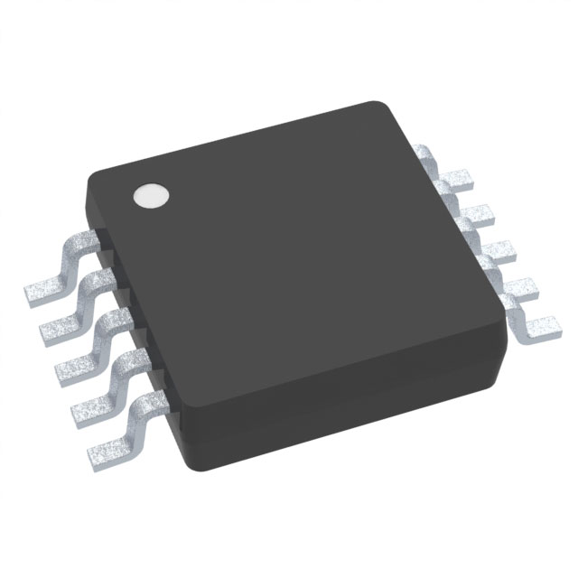
OPA2625IDGSR
OP Amps, Buffer Amps ICs


- 1+
- $5.47474
- $5.47
- 10+
- $5.35219
- $53.52
- 30+
- $5.27105
- $158.13

.png?x-oss-process=image/format,webp/resize,p_30)


OPA2625IDGSR Description
The Texas Instruments OPA2625IDGSR is a high-performance, low-noise, precision operational amplifier (op-amp) designed for a variety of applications that require high accuracy and low noise performance. Here is a brief description of the OPA2625IDGSR, its features, and potential applications:
Description:
The OPA2625IDGSR is a member of the OPA2x family of operational amplifiers, which are known for their precision and low-noise characteristics. This specific model is offered in a compact 8-pin SOIC (Small Outline Integrated Circuit) package, making it suitable for a wide range of electronic systems where space is at a premium.
Features:
- Low Input Noise: The OPA2625 is designed with a low input voltage noise of 3.5 nV/√Hz, making it ideal for applications where signal integrity is critical.
- Low Offset Drift: It has a low input offset voltage drift of 0.5 µV/°C, which is beneficial for maintaining accuracy over temperature changes.
- High Input Impedance: The op-amp has high input impedance, which is desirable for applications where the source impedance is high.
- Low Output Noise: The OPA2625IDGSR has a low output noise level, which is crucial for applications requiring a clean output signal.
- Precision: It offers precision performance with a low input offset voltage of typically 100 µV max.
- Wide Supply Voltage Range: The device can operate over a supply voltage range of ±2.5V to ±18V, making it versatile for different power supply configurations.
- Short Circuit Protection: It includes internal protection against output short circuits, which can help prevent damage to the device during fault conditions.
- High Slew Rate: A slew rate of 7 V/µs allows the op-amp to handle fast-changing input signals.
Applications:
- Audio Equipment: Due to its low noise characteristics, the OPA2625 is well-suited for use in high-fidelity audio amplifiers and preamplifiers.
- Medical Instruments: In medical equipment where signal integrity and precision are crucial, such as in hearing aids or medical monitoring devices.
- Sensor Conditioning: For conditioning signals from sensors in industrial or automotive applications where accurate signal processing is required.
- Data Acquisition Systems: In systems that require high-resolution signal processing, such as in precision instrumentation and data acquisition systems.
- Strains and Load Cells: For amplifying and filtering signals from strain gauges and load cells in measurement and control systems.
- Photodiode Amplification: In applications where photodiodes are used to convert light into electrical signals, such as in optical sensing and spectroscopy.
The OPA2625IDGSR is a versatile operational amplifier that can be integrated into a wide range of electronic systems where precision and low-noise performance are paramount.
Tech Specifications
OPA2625IDGSR Documents
Download datasheets and manufacturer documentation for OPA2625IDGSR
 OPA625, OPA2625 Datasheet
  OPA625, OPA2625 Datasheet
 Shopping Guide


.png?x-oss-process=image/format,webp/resize,h_32)


