
 German
 Japanese
 Portuguese
 Korea
Korea
 Mexico
 Dutch
Dutch


Texas Instruments
OPA2727AIDRBR

Why Choose Us?
Professional Platform
B2B & B2C purchasingDelivery at full speed
1-2 days deliveryWide variety
Original manufacturers365 days guarantee
Responsible quality
.png)


Tech Specifications
OPA2727AIDRBR Description
OPA2727AIDRBR Description
The OPA2727AIDRBR is a high-performance CMOS operational amplifier designed by Texas Instruments, featuring dual circuits in an 8-lead SON (Small Outline No-lead) package. This IC is optimized for low power consumption and high performance, making it suitable for a variety of applications. The OPA2727AIDRBR operates within a supply voltage range of 3.5 V to 12 V, ensuring flexibility in power supply requirements. It boasts a gain bandwidth product of 20 MHz, a slew rate of 30 V/µs, and a low input bias current of 85 pA. The device also features a low input offset voltage of 15 µV, contributing to its high precision and stability.
OPA2727AIDRBR Features
- Amplifier Type: CMOS, ensuring low power consumption and high efficiency.
- Supply Voltage Range: 3.5 V to 12 V, providing flexibility for various power supply configurations.
- Gain Bandwidth Product: 20 MHz, enabling high-frequency applications.
- Slew Rate: 30 V/µs, ensuring fast transient response and minimal distortion.
- Input Bias Current: 85 pA, minimizing the impact of input current on the signal.
- Input Offset Voltage: 15 µV, contributing to high accuracy and stability.
- Supply Current: 4.3 mA per channel, ensuring low power consumption.
- Output Current per Channel: 40 mA, capable of driving moderate loads.
- Number of Circuits: Dual, allowing for compact and efficient designs.
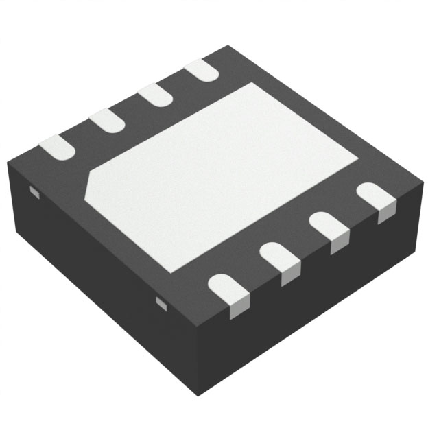
- Package Type: 8-lead SON, suitable for surface mount applications.
- Moisture Sensitivity Level (MSL): Level 3 (168 hours), ensuring reliability in manufacturing processes.
- Compliance: RoHS3 compliant and REACH unaffected, meeting environmental and regulatory standards.
OPA2727AIDRBR Applications
The OPA2727AIDRBR is ideal for applications requiring high performance and low power consumption. Its dual-channel design makes it suitable for compact and efficient designs. Key applications include:
- Signal Conditioning: High-precision signal amplification and conditioning in industrial and medical equipment.
- Analog-to-Digital Conversion: Driving ADCs with high slew rates and low offset voltage.
- Audio Processing: High-fidelity audio amplification and processing.
- Data Acquisition Systems: Precision signal amplification in data acquisition systems.
- Instrumentation: High-precision measurement and control systems.
Conclusion of OPA2727AIDRBR
The OPA2727AIDRBR from Texas Instruments is a versatile and high-performance CMOS operational amplifier, offering a combination of low power consumption, high precision, and fast response. Its dual-channel design and compact 8-lead SON package make it suitable for a wide range of applications, from signal conditioning to audio processing. The device's compliance with RoHS3 and REACH standards ensures it meets environmental and regulatory requirements. The OPA2727AIDRBR is an excellent choice for designers seeking a reliable and efficient solution for their analog circuits.
FAQ
Not available to buy online? Want the lower wholesale price? Please Send RFQ to get best price, we will respond immediately


.png?x-oss-process=image/format,webp/resize,h_32)


