
Texas Instruments
OPA2846ID
OP Amps, Buffer Amps ICs


.png?x-oss-process=image/format,webp/resize,p_30)


OPA2846ID Description
OPA2846ID Description
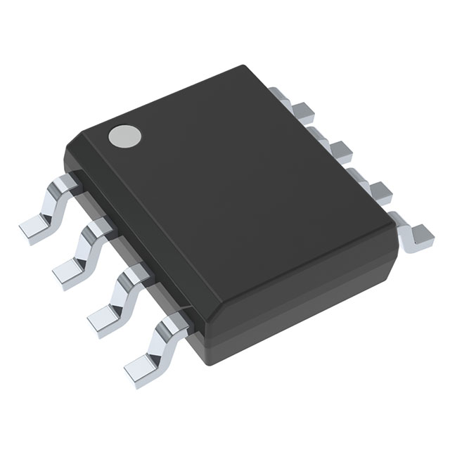
The OPA2846ID is a high-performance, dual-channel voltage feedback amplifier designed for demanding applications requiring exceptional speed and precision. Manufactured by Texas Instruments, this IC is part of the Linear Amplifiers(ICs) category and is housed in an 8SOIC package. The OPA2846ID features a wide supply voltage range, from a minimum of 5 V to a maximum of 12 V, making it suitable for various power supply configurations. Its gain bandwidth product of 1.65 GHz ensures high-frequency performance, while the 600V/µs slew rate guarantees rapid response times. The amplifier's input bias current is a low 10 µA, minimizing the impact of input loading on signal sources. With a supply current of 25.2mA and an output current per channel of 80 mA, the OPA2846ID can drive substantial loads efficiently. The input offset voltage is tightly controlled at 150 µV, contributing to high accuracy in signal processing.
OPA2846ID Features
- High Gain Bandwidth Product: The 1.65 GHz gain bandwidth product allows the OPA2846ID to handle high-frequency signals with minimal distortion, making it ideal for applications requiring wide bandwidth and fast transient response.
- High Slew Rate: The 600V/µs slew rate ensures that the amplifier can quickly respond to large signal changes, reducing settling time and improving overall system performance.
- Low Input Bias Current: The 10 µA input bias current minimizes the loading effect on the signal source, preserving signal integrity and reducing errors in high-impedance circuits.
- Wide Supply Voltage Range: The 5 V to 12 V supply voltage range provides flexibility in power supply design, accommodating both low-voltage and higher-voltage systems.
- High Output Current: The 80 mA output current per channel allows the OPA2846ID to drive significant loads, making it suitable for applications requiring high output power.
- Low Input Offset Voltage: The 150 µV input offset voltage ensures high accuracy in signal processing, minimizing errors and improving the overall performance of precision circuits.
- Surface Mount Packaging: The OPA2846ID is available in a surface mount package, facilitating easy integration into compact and high-density PCB designs.
- Compliance and Reliability: The OPA2846ID is REACH unaffected and RoHS3 compliant, ensuring environmental sustainability and regulatory compliance. The moisture sensitivity level (MSL) of 2 (1 Year) provides robustness against environmental factors.
OPA2846ID Applications
The OPA2846ID is well-suited for a variety of applications that demand high-speed signal processing and precision. Some specific use cases include:
- High-Speed Data Converters: The OPA2846ID's high bandwidth and slew rate make it ideal for driving high-speed ADCs and DACs, ensuring accurate and rapid signal conversion.
- RF and Microwave Systems: In RF and microwave applications, the OPA2846ID can be used for signal conditioning and amplification, providing the necessary bandwidth and speed to handle high-frequency signals.
- Medical Imaging Equipment: The precision and speed of the OPA2846ID are crucial for medical imaging applications, where accurate and rapid signal processing is essential for high-quality imaging.
- Industrial Automation: The OPA2846ID can be used in industrial automation systems for signal processing and control, providing the high performance needed for real-time applications.
- Communication Systems: In communication systems, the OPA2846ID can be used for signal amplification and conditioning, ensuring reliable and high-speed data transmission.
Conclusion of OPA2846ID
The OPA2846ID from Texas Instruments is a versatile and high-performance dual-channel voltage feedback amplifier that excels in applications requiring high speed and precision. Its wide supply voltage range, high gain bandwidth product, and high slew rate make it a standout choice for demanding applications. The low input bias current and low input offset voltage ensure high accuracy and minimal signal distortion. With its surface mount packaging and compliance with environmental regulations, the OPA2846ID is a reliable and efficient solution for modern electronic designs. Whether used in high-speed data converters, RF and microwave systems, medical imaging equipment, industrial automation, or communication systems, the OPA2846ID delivers exceptional performance and reliability.
Tech Specifications
OPA2846ID Documents
Download datasheets and manufacturer documentation for OPA2846ID
 OPA2846
  OPA2846
  Design 25/Feb/2022
 Shopping Guide


.png?x-oss-process=image/format,webp/resize,h_32)


