
 German
 Japanese
 Portuguese
 Korea
Korea
 Mexico
 Dutch
Dutch


Texas Instruments
OPA2890IDGST

Why Choose Us?
Professional Platform
B2B & B2C purchasingDelivery at full speed
1-2 days deliveryWide variety
Original manufacturers365 days guarantee
Responsible quality
.png)


Tech Specifications
OPA2890IDGST Description
OPA2890IDGST Description
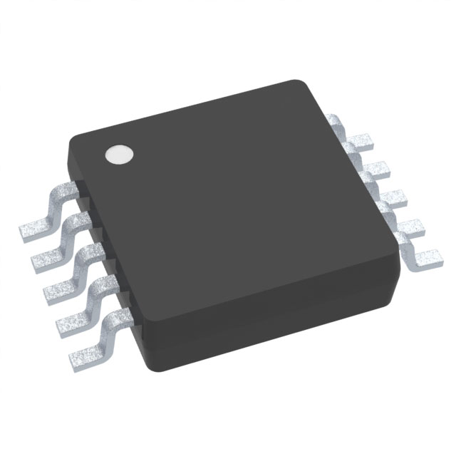
The OPA2890IDGST is a high-performance dual-channel operational amplifier designed by Texas Instruments, featuring a voltage feedback architecture. This IC is optimized for high-speed signal processing and offers a wide supply voltage range from 3 V to 12 V, making it suitable for a variety of power supply configurations. The OPA2890IDGST is housed in a 10-pin VSSOP package, which is ideal for surface-mount applications, ensuring compact and efficient integration into modern electronic designs.
OPA2890IDGST Features
- High Gain Bandwidth Product: The OPA2890IDGST boasts a gain bandwidth product of 120 MHz, enabling it to handle high-frequency signals with minimal distortion. This feature is crucial for applications requiring fast signal processing and wide bandwidth.
- High Slew Rate: With a slew rate of 400 V/µs, the OPA2890IDGST can quickly respond to large signal changes, ensuring accurate and timely signal reproduction. This high slew rate makes it ideal for applications involving rapid signal transitions.
- Low Input Bias Current: The input bias current is a mere 100 nA, which minimizes the loading effect on the input signal source, ensuring high input impedance and minimal signal degradation.
- Low Input Offset Voltage: The input offset voltage is maintained at 2 mV, ensuring high accuracy and stability in signal amplification.
- High Output Current Capability: Each channel can deliver up to 40 mA of output current, providing robust performance and the ability to drive heavy loads.
- Wide Supply Voltage Range: The operational amplifier can function effectively within a supply voltage range of 3 V to 12 V, offering flexibility in power supply design.
- Compliance and Reliability: The OPA2890IDGST is REACH unaffected and RoHS3 compliant, ensuring environmental safety and reliability. It also has a moisture sensitivity level (MSL) of 2 (1 Year), making it suitable for various manufacturing environments.
OPA2890IDGST Applications
The OPA2890IDGST is well-suited for a range of high-speed, high-precision applications, including:
- High-Speed Signal Processing: Ideal for applications requiring fast and accurate signal processing, such as in high-speed data acquisition systems.
- Video Signal Processing: Suitable for video signal amplification and processing, ensuring high-quality video output with minimal latency.
- RF and Microwave Applications: The high bandwidth and slew rate make it suitable for RF and microwave applications where fast signal transitions are critical.
- Instrumentation and Control Systems: The low input bias current and offset voltage ensure high accuracy and stability, making it ideal for precision instrumentation and control systems.
- Medical Equipment: The high performance and reliability make it suitable for medical imaging and diagnostic equipment where precision and speed are paramount.
Conclusion of OPA2890IDGST
The OPA2890IDGST from Texas Instruments is a versatile and high-performance dual-channel operational amplifier that excels in high-speed and high-precision applications. Its wide supply voltage range, low input bias current, and high slew rate make it a standout choice for demanding applications in various industries. Whether used in high-speed data acquisition, video signal processing, or precision instrumentation, the OPA2890IDGST delivers reliable performance and superior signal integrity. Its compliance with environmental standards and robust manufacturing specifications further enhance its appeal for modern electronic designs.
FAQ
Not available to buy online? Want the lower wholesale price? Please Send RFQ to get best price, we will respond immediately


.png?x-oss-process=image/format,webp/resize,h_32)


