Texas Instruments_OPA333AIDBVR

Texas Instruments
OPA333AIDBVR  
OP Amps, Buffer Amps ICs

Texas Instruments
OPA333AIDBVR
687-OPA333AIDBVR
Ersa
Texas Instruments-OPA333AIDBVR-datasheets-10558284.pdf
IC OPAMP ZER-DRIFT 1CIRC SOT23-5
In Stock : 6373

Not available to buy online? Want the lower wholesale price? Please Send RFQ to get best price, we will respond immediately

QUICK RFQ
ADD TO RFQ LIST
ersa FreeSample ersa flow
  • Quantity
  • Unit Price
  • Ext. Price
    • 1+
    • $0.59119
    • $0.59
    • 10+
    • $0.51005
    • $5.1
    • 30+
    • $0.45209
    • $13.56
    • 100+
    • $0.40572
    • $40.57
    • 500+
    • $0.33120
    • $165.6
    • 1000+
    • $0.32292
    • $322.92
    ADD TO CART
    QUICK ORDER
    $0.59119    $0.59
    ISO9001
    Quality Policy
    ISO45001
    ISO14001

    OPA333AIDBVR Description

    The OPA333AIDBVR is a precision operational amplifier (op-amp) from Texas Instruments. It is designed for high-precision applications and offers a wide range of features that make it suitable for a variety of applications.

    Description:

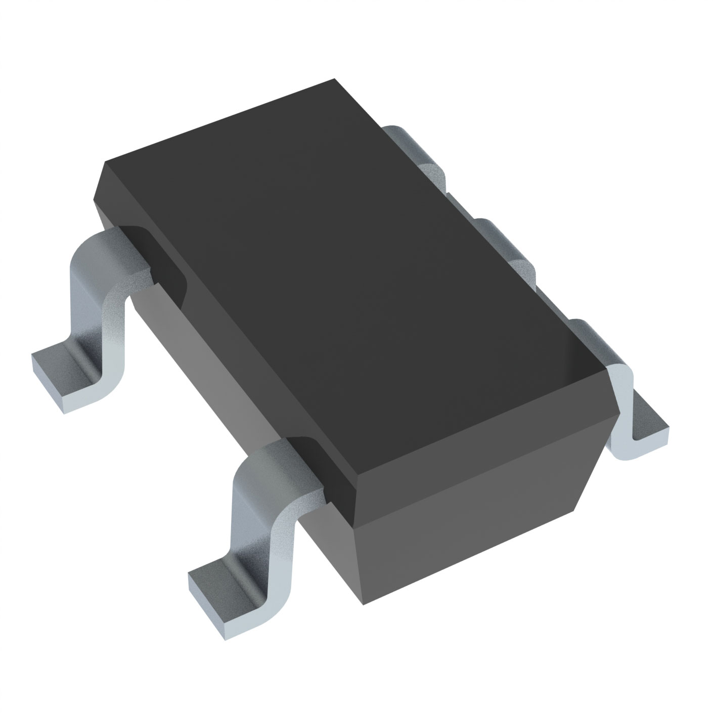
    The OPA333AIDBVR is a low-noise, low-offset, precision operational amplifier that operates from a single supply voltage as low as 2.5V. It is available in a small 8-pin SOIC package, making it ideal for use in compact and space-constrained applications.

    Features:

    1. Low input offset voltage: The OPA333AIDBVR has an input offset voltage as low as 100µV, making it suitable for precision applications where accurate amplification is required.
    2. Low input bias current: The input bias current is as low as 2pA, which helps to minimize errors in high-impedance circuits.
    3. Low noise: The OPA333AIDBVR has a low input voltage noise of 4.3nV/√Hz, making it suitable for use in applications that require low-noise amplification.
    4. Wide supply voltage range: The op-amp can operate from a supply voltage as low as 2.5V, making it suitable for use in low-voltage applications.
    5. High output current: The OPA333AIDBVR can provide an output current of up to ±90mA, making it suitable for driving high-current loads.

    Applications:

    The OPA333AIDBVR is suitable for a variety of high-precision applications, including:

    1. Strain gauge amplifiers: The low input offset voltage and low noise make it ideal for use in strain gauge amplifiers, where accurate measurements are critical.
    2. Medical instrumentation: The low input bias current and low noise make it suitable for use in medical instrumentation, where accurate and reliable measurements are required.
    3. Data acquisition systems: The low noise and high output current make it suitable for use in data acquisition systems, where accurate and reliable amplification is required.
    4. Audio equipment: The low noise and low distortion characteristics make it suitable for use in audio equipment, where high-quality sound reproduction is required.
    5. Industrial control systems: The wide supply voltage range and high output current make it suitable for use in industrial control systems, where reliable and accurate amplification is required.

    In summary, the OPA333AIDBVR is a precision operational amplifier from Texas Instruments that offers a wide range of features, including low input offset voltage, low input bias current, low noise, and a wide supply voltage range. It is suitable for use in a variety of high-precision applications, including strain gauge amplifiers, medical instrumentation, data acquisition systems, audio equipment, and industrial control systems.

    Tech Specifications

    Number of Channels per Chip
    Unit Weight
    Power Supply Type
    Rail-to-rail
    Product
    PPAP
    Gain Bandwidth Product
    Automotive
    Maximum Input Offset Current (uA)
    RoHS
    REACH Status
    Input common mode headroom (to negative supply) (typ) (V)
    Operating temperature range (°C)
    PSRR - Power Supply Rejection Ratio
    Current - Supply
    Output swing headroom (to negative supply) (typ) (V)
    Standard Package Name
    Shut Down Support
    Mounting
    Minimum Single Supply Voltage (V)
    Iout (typ) (A)
    Manufacturer Type
    Package
    Minimum CMRR (dB)
    Total supply voltage (+5 V = 5, ±5 V = 10) (max) (V)
    GBW (typ) (MHz)
    en - Input Voltage Noise Density
    Output Type
    Vos - Input Offset Voltage
    Minimum Dual Supply Voltage
    Minimum CMRR Range (dB)
    Process Technology
    Typical Gain Bandwidth Product (MHz)
    Package Height
    Maximum Operating Temperature
    Ib - Input Bias Current
    Width
    RoHS Status
    Number of channels
    Iq per channel (typ) (mA)
    Minimum Operating Temperature
    Voltage - Input Offset
    Type
    Vos (offset voltage at 25°C) (max) (mV)
    Length
    Operating Supply Voltage
    Output Current per Channel
    Part Status
    Supply Type
    Lead finish / Ball material
    Number of Circuits
    Package Width
    GBP - Gain Bandwidth Product
    Voltage - Supply Span (Max)
    Maximum Input Offset Voltage (mV)
    Product Status
    Current - Input Bias
    Rail to Rail
    Supplier Package
    Package / Case
    Number of Channels
    Typical Voltage Gain (dB)
    Technology
    EU RoHS
    Carrier
    Amplifier Type
    Maximum Dual Supply Voltage (V)
    Input common mode headroom (to positive supply) (typ) (V)
    Moisture Sensitivity Level (MSL)
    Operating Temperature
    Architecture
    Typical Slew Rate (V/us)
    Output swing headroom (to positive supply) (typ) (V)
    ECCN
    MSL rating / Peak reflow
    Mounting Type
    Pin Count
    In - Input Noise Current Density
    Minimum PSRR (dB)
    Shutdown
    Vcm - Common Mode Voltage
    Voltage - Supply Span (Min)
    Lead Shape
    HTSUS
    Pins
    Current - Output / Channel
    USHTS
    Maximum Dual Supply Voltage
    PCB changed
    HTS
    Voltage Gain dB
    Rating
    ECCN (US)
    Total supply voltage (+5 V = 5, ±5 V = 10) (min) (V)
    Supplier Device Package
    Supply Voltage - Min
    Minimum Operating Temperature (°C)
    Maximum Operating Temperature (°C)
    Operating Supply Current
    SR - Slew Rate
    Mfr
    Height
    Features
    CMRR (typ) (dB)
    Supply Voltage - Max
    Offset drift (typ) (µV/°C)
    Mounting Style
    Input Type
    Maximum Input Bias Current (uA)
    Typical Noninverting Input Current Noise Density (pA/rtHz)
    Slew Rate
    Package Length
    Minimum Dual Supply Voltage (V)
    Vn at 1 kHz (typ) (nV√Hz)
    CMRR - Common Mode Rejection Ratio
    REACH
    Series
    Maximum Single Supply Voltage (V)
    Slew rate (typ) (V/µs)
    Base Product Number
    Input bias current (max) (pA)

    OPA333AIDBVR Documents

    Download datasheets and manufacturer documentation for OPA333AIDBVR

    Ersa Mult Dev A/T Chgs 30/Aug/2023      
    Ersa OPA333, 2333 Datasheet      
    Ersa OPA333, 2333 Datasheet      
    Ersa OPA2317/OPA317/TLV2333 07/Dec/2016       OPAYYY/TLVYYY 05/Dec/2016      

    Shopping Guide

    Payment Methods
    Payment Methods include Prepayment TT (bank transfer), Western Union, and PayPal. Customers are responsible for shipping costs, bank charges, customs duties and taxes.
    Shipping Rate
    Shipments are made once a day around 5pm, excluding Sundays. Once shipped, the estimated delivery time is usually 5-7 business days, depending on the courier you choose.
    Delivery Methods
    Provide DHL, FedEx, UPS, EMS, SF Express and Registered Airmail International Delivery Service