
Texas Instruments
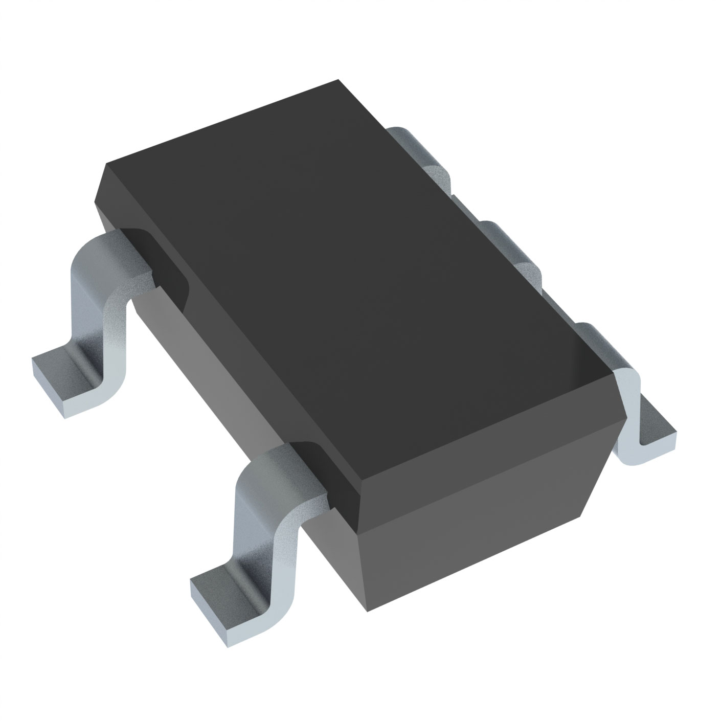
OPA348AQDBVRQ1
OP Amps, Buffer Amps ICs


.png?x-oss-process=image/format,webp/resize,p_30)


OPA348AQDBVRQ1 Description
The Texas Instruments OPA348AQDBVRQ1 is a high-performance, low-noise, low-power, dual operational amplifier (op-amp) designed for a wide range of precision applications. Here is a description of the model, its features, and potential applications:
Model: OPA348AQDBVRQ1
Description:
The OPA348 is a dual operational amplifier that combines excellent DC and AC performance with low power consumption. It is housed in a compact 8-pin VSSOP package, making it suitable for space-constrained applications.
Features:
- Low Input Voltage Noise: The OPA348 offers low input voltage noise of 2.2 nV/√Hz, which is beneficial for applications requiring high signal-to-noise ratios.
- Low Offset Drift: It has a low input offset voltage drift of 0.2 µV/°C, contributing to its precision performance.
- Low Power Consumption: The OPA348 consumes only 330 µA per amplifier, making it suitable for battery-powered applications.
- High Input Impedance: With an input impedance of 1.8 GΩ, it can drive high impedance loads without significant loading effects.
- Wide Supply Voltage Range: The device can operate with supply voltages ranging from ±2.5V to ±18V, providing flexibility in system design.
- Short Circuit Protection: It includes internal protection against output short circuits.
- Lead-Free Packaging: The OPA348AQDBVRQ1 is available in lead-free packages, which are RoHS compliant.
Applications:
- Precision ADC Drivers: The OPA348's low noise and low distortion characteristics make it ideal for driving high-resolution analog-to-digital converters (ADCs).
- Medical Instruments: Its precision and low noise performance are suitable for medical equipment, such as ultrasound systems and patient monitoring devices.
- High-Resolution Audio Systems: The OPA348 can be used in professional and consumer audio equipment to maintain high-fidelity audio signals.
- Strains Gauges Amplification: Due to its low noise and low drift, it is suitable for amplifying signals from strain gauges in industrial and automotive applications.
- Battery Monitors: The low power consumption of the OPA348 makes it an excellent choice for battery monitoring circuits in portable electronic devices.
- Sensor Conditioning: It can be used to amplify and condition signals from various types of sensors, such as temperature, pressure, or humidity sensors.
- Precision Instrumentation: The OPA348 is suitable for precision instrumentation applications where low noise, low drift, and low power are critical.
The OPA348AQDBVRQ1 is a versatile operational amplifier that can be integrated into a wide range of applications requiring high precision and low power consumption. Its combination of performance and flexibility makes it a popular choice among engineers and designers.
Tech Specifications
OPA348AQDBVRQ1 Documents
Download datasheets and manufacturer documentation for OPA348AQDBVRQ1
 OPA348-Q1, 2348-Q1, 43.48-Q1
  OPA348-Q1, 2348-Q1, 43.48-Q1
 Shopping Guide


.png?x-oss-process=image/format,webp/resize,h_32)


